平台:Code Composer Studio 10.3.1
MSP430F5529 LaunchPad™ Development Kit
(MSP‑EXP430F5529LP)
硬知识
模数转换概述
在MSP430单片机的实时控制和智能仪表等实际应用系统中,常常会遇到连续变化的物理量,如温度、流量、压力和速度等。利用传感器把这些物理量检测出来,转换为模拟电信号,再经过模数转换模块(ADC)转换成数字量,模拟量才能够被MSP430单片机处理和控制。
1.模数转换基本过程
首先连续时间输入信号x(t)输入ADC的采样保持器中,ADC每隔Ts(采样周期)读出一次x(t)的采样值,对此采样值进行量化。量化的过程是将此信号转换成离散时间、离散幅度的多电平信号。从数学角度理解,量化是把一个连续幅度值的无限数集合映射到一个离散幅度值的有限数集合。在进行ADC转换时,必须把采样电压表示为某个规定的最小数量单位的整数倍,所取的最小数量单位叫做量化单位,用Δ表示。显然,数字信号最低有效位(LSB)的1所代表的数量大小就等于Δ。把量化的结果用代码表示出来,这个过程称为编码。这些代码就是ADC转换的输出结果。
2.ADC的位数
ADC的位数为ADC模块采样转换后输出代码的位数。例如,一个12位的ADC模块,采样转换后的代码即为12位,表示数值的取值范围为0~4095。
3.分辨率
分辨率表示输出数字量变化的一个相邻数码所需输入模拟电压的变化量。它定义为转换器的满刻度电压与2n的比值,其中n为ADC的位数。因此,分辨率与ADC的位数有关。例如,一个8位ADC模块的分辨率为满刻度电压的1/256。如果满刻度输入电压为5V,该ADC模块的分辨率即为5V/256=20mV。分辨率代表了ADC模块对输入信号的分辨能力,一般来说,ADC模块位数越高,数据采集的精度就越高。
4.量化误差
量化误差是由于用有限数字对模拟数值进行离散取值(量化)而引起的误差。因此,量化误差理论上为一个单位分辨率,即1/2LSB。量化误差是无法消除的,但是,通过提高分辨率可以减少量化误差。
5.采样周期
采样周期是每两次采样之间的时间间隔。采样周期包括采样保持时间和转换时间。采样保持时间是指ADC模块完成一次采样和保持的时间,转换时间是指ADC模块完成一次模数转换所需要的时间。在MSP430单片机的ADC12模块中,采样保持时间可通过控制寄存器进行设置,而转换时间一般需要13个ADCCLK的时间。
6.采样频率
采样频率,也称为采样速率或者采样率,定义为每秒从连续信号中提取并组成离散信号的采样个数,单位为赫兹(Hz)。采样频率的倒数是采样周期。为了确定对一个模拟信号的采样频率,在此简单介绍采样定理。采样定理又称香农采样定理或者奈奎斯特采样定理,即在进行模数信号的转换过程中,当采样频率fs.max大于信号中最高频率分量fmax的2倍时(fs.max≥2fmax),采样之后的数字信号能保留原始信号中的信息。在一般应用中,采样频率应为被采样信号中最高频率的5~10倍。
7.采样保持电路
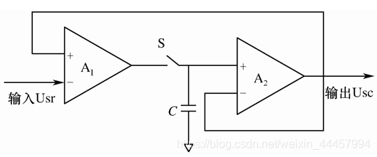
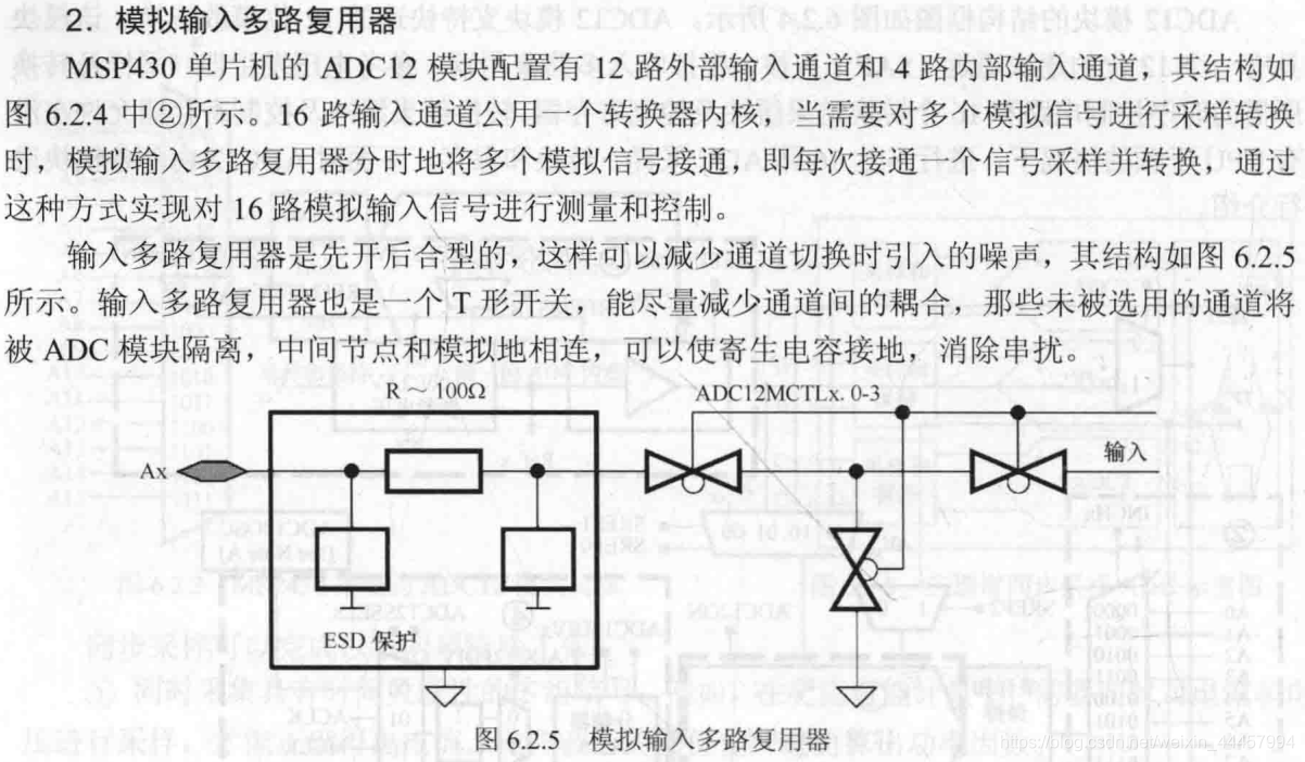
采样保持电路(S/H或者SH)是模数转换系统中的一种重要电路,其作用是采集模拟输入电压在某一时刻的瞬时值,并在模数转换器进行转换期间保持输出电压不变,以供模数转换。该电路存在的原因在于模数转换需要一定时间,在转换过程中,如果送给ADC的模拟量发生变化,就不能保证采样的精度。为了简单起见,在此只分析单端输入ADC的采样保持电路,如图所示。
采样保持电路有两种工作状态:采样状态和保持状态。当控制开关S闭合时,输出跟随输入变化,称为采样状态;当控制开关S断开时,由保持电容C维持该电路的输出不变,称为保持状态。
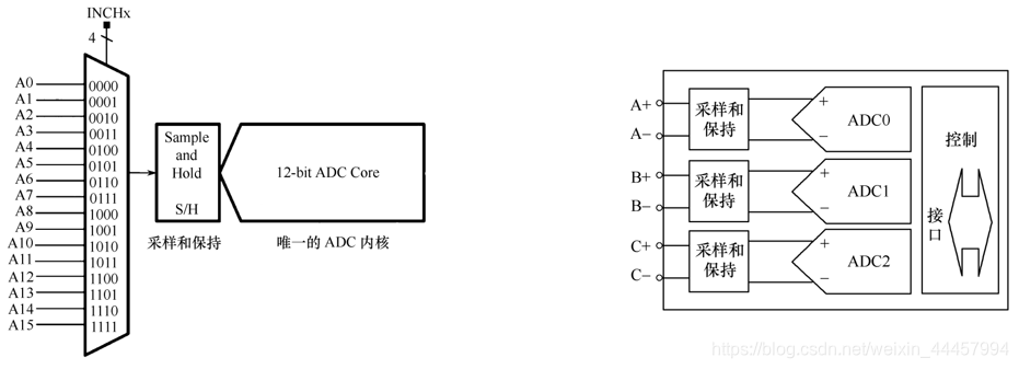
8.多通道同步采样和分时复用
大多数单片机都集成了8个以上的ADC通道,这些单片机内部的ADC模块大多都是多通道分时复用的结构,其内部其实只有一个ADC内核,依靠增加模拟开关的方法轮流使用ADC内核,所以可以有多个ADC的输入通道。MSP430单片机也采用这种结构,如左图所示。
同步采样ADC实际就是多个完整独立的ADC。如右图所示为三通道同步采样ADC的示意图。每一组通道都有各自独立的采样保持电路和ADC内核,3个ADC模块共用控制电路和输入/输出接口。
MSP430单片机ADC12模块介绍
ADC12模块的特性有:
高达200ksps的最大转换率;
无数据丢失的单调的12位转换器;
采样周期可由软件或定时器编程控制的采样保持功能;
软件或定时器启动转换;
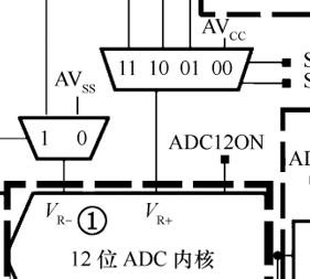
可通过软件选择片内参考电压(MSP430F54xx:1.5V或2.5V,其他芯片:1.5V、2.0V或2.5V,注意此处只限MSP430F5xx/6xx系列单片机);
可通过软件选择内部或外部参考电压;
高达12路可单独配置的外部输入通道;
可为内部温度传感器、AVCC和外部参考电压分配转换通道;
正或负参考电压通道可独立选择;
转换时钟源可选;
具有单通道单次、单通道多次、序列通道单次和序列通道多次的转换模式;
ADC内核和参考电压都可独立关闭;
具有18路快速响应的ADC中断;
具有16个转换结果存储寄存器。
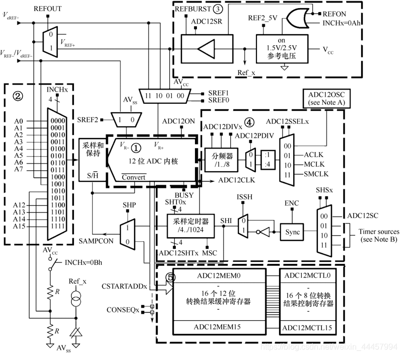
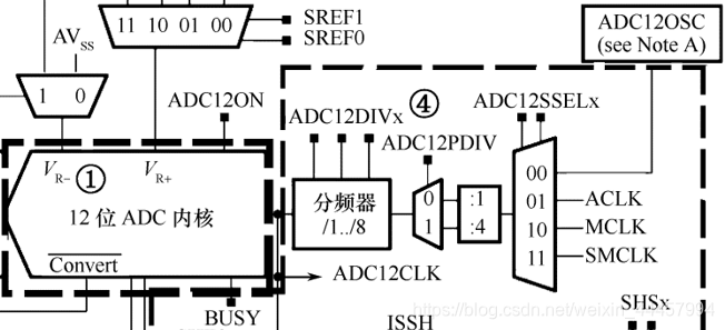
ADC12模块的结构框图如图所示。ADC12模块支持快速的12位模数转换。该模块具有一个12位的逐次逼近(SAR)内核、模拟输入多路复用器、参考电压发生器、采样及转换所需的时序控制电路和16个转换结果缓冲及控制寄存器。转换结果缓冲及控制寄存器允许在没有CPU干预的情况下,进行多达16路ADC采样、转换和保存。
MSP430单片机ADC12模块操作
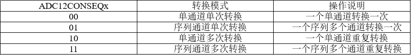
ADC12的转换模式
ADC12模块有4种转换模式,可以通过CONSEQx控制位进行选择,具体转换模式说明如表所示。
(1)单通道单次转换模式
该模式对单一通道实现单次转换。模数转换结果被写入由CSTARTADDx位定义的存储寄存器ADC12MEMx中。单通道单次转换的流程图如图所示。当用户利用软件使ADC12SC启动转换时,下一次转换可以通过简单地设置ADC12SC位来启动。当有其他任何触发源用于转换时,ADC12ENC位必须在等待触发信号之前置位(上升沿)。其他的采样输入信号将在ADC12ENC复位并置位之前被忽略。
(2)序列通道单次转换模式
该模式对序列通道做单次转换。ADC12转换结果将顺序写入由CSTARTADDx位定义的以ADCMEMx开始的转换存储器中。当由ADC12MCTLx寄存器中ADC12EOS位定义的最后一个通道转换完成之后,整个序列通道转换完成。序列通道单次转换的流程图如图所示。当使用ADC12SC位启动转换时,下一次转换可以通过简单地设置ADC12SC位来启动。当有其他任何触发源用于开始转换,ADC12ENC位必须在等待触发信号前置位(上升沿)。其他的采样输入信号将在ADC12ENC复位并置位之前被忽略。
(3)单通道多次转换模式
单通道多次转换模式是在选定的通道上进行多次转换。ADC转换的结果被存入由CSTARTADDx位定义的ADC12MEMx寄存器中。在这种转换模式下,当每次转换完成后CPU必须读取ADC12MEMx寄存器的值,否则在下一次转换中,ADC12MEMx寄存器的值会被覆盖。单通道多次转换模式的流程图如图所示。在此模式下,若复位ADC12ENC位,则在当前转换完成之后,转换将立即停止。同时设置CONSEQx=0和ADC12ENC=0,也可以立即停止当前的转换,但是,转换结果是不可靠的。
(4)序列通道多次转换模式
序列通道多次转换模式用来进行多通道的连续转换。ADC12转换结果将顺序写入由CSTARTADDx位定义的以ADCMEMx开始的存储器中。当由ADC12MCTLx寄存器中ADC12EOS位定义的最后一个通道转换完成之后,一次序列通道转换完成,触发信号会触发下一次序列通道转换。序列通道多次转换模式的流程图如图所示。

采样和转换
当采样触发信号SHI出现上升沿时将启动模数转换。SHI信号源可以通过SHSx位进行定义,有4种选择:ADC12SC、Timer_A.OUT1、Timer_B.OUT0、Timer_B.OUT1。ADC12支持8位、10位及12位分辨率模式,可以通过ADC12RES控制位进行选择,模数转换分别需要9、11及13个ADC12CLK周期。采样输入信号的极性用ISSH控制位来选择。采样转换信号SAMPCON可以来自于采样输入信号SHI或采样定时器,能够控制采样的周期及转换的开始。当SAMPCON信号为高电平时采样被激活,SAMPCON的下降沿将触发模数转换。ADC12SHP定义了两种不同的采样时序方法:扩展采样时序模式和脉冲采样时序模式。
转换存储器
典型的模数操作通常用中断请求的方式来通知ADC转换的结束,并需要在下一次ADC执行前将转换结果转存到另一位置。ADC12中的16个转换存储缓冲寄存器(ADC12MEMx)使得ADC可以进行多次转换而不需要软件干预,这一点提高了系统性能,也减少了软件开销。
ADC12模块的每个ADC12MEMx缓冲寄存器都可通过相关的ADC12MCTLx控制寄存器来配置,为转换存储提供了很大的灵活性。SREFx控制位定义了参考电压,INCHx控制位选择输入通道。当使用序列通道转换模式时,ADC12EOS控制位定义了转换序列的结束。
使用片内集成温度传感器
如果需要使用MSP430单片机片内的温度传感器,用户可以选择模拟输入通道INCHx=1010。与选择外部输入通道一样,需要进行其他寄存器的配置,包括参考电压选择、转换存储寄存器选择等。温度传感器典型的转换函数如图6.2.12所示,该转换函数仅仅作为一个示例,实际的参数可以参考具体芯片的数据手册。当使用温度传感器时,采样周期必须大于30ms。温度传感器的偏移误差比较大,在大多数实际应用中需要进行校准。选择温度传感器会自动地开启片上参考电压发生器作为温度传感器的电源。但是,它不会使能VREF+输出或者影响作为模数转换的参考电压设置,温度传感器的参考电压设置与其他通道相同。
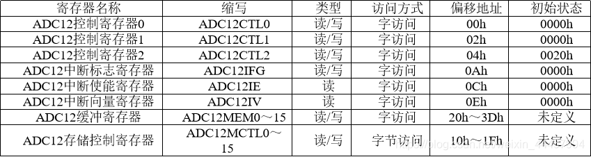
ADC12模块寄存器
ADC_12A API (机翻)
ADC_12A API被分成三组函数:
处理初始化和转换的函数,
处理中断的函数,
处理ADC_12A的辅助功能的函数。
处理初始化和转换的函数
ADC12_A_init(uint16_t baseAddress, uint16_t sampleHoldSignalSourceSelect, uint8_t clockSourceSelect, uint16_t clockSourceDivider)
//初始化ADC12_A模块
ADC12_A_configureMemory(uint16_t baseAddress, ADC12_A_configureMemoryParam ∗param)
//配置所选内存缓冲区的控件
ADC12_A_setupSamplingTimer(uint16_t baseAddress, uint16_t clockCycleHoldCountLowMem, uint16_t clockCycleHoldCountHighMem, uint16_t multipleSamplesEnabled)
//设置并启用采样定时器脉冲模式
ADC12_A_disableSamplingTimer(uint16_t baseAddress)
//禁用采样定时器脉冲模式
ADC12_A_startConversion(uint16_t baseAddress, uint16_t startingMemoryBufferIndex, uint8_t conversionSequenceModeSelect)
//使能/开始模数转换
ADC12_A_disableConversions(uint16_t baseAddress, bool preempt)
//禁止ADC转换任何信号
ADC12_A_getResults(uint16_t baseAddress, uint8_t memoryBufferIndex)
//A Signed Integer of the contents of the specified memory buffer
ADC12_A_isBusy(uint16_t baseAddress)
//返回ADC12_A核心的忙碌状态。
参数
baseAddress
ADC12_A_BASE
sampleHoldSignalSourceSelect
/*
is the signal that will trigger a sample-and-hold for an input
signal to be converted. This parameter is device specific and
sources should be found in the device's datasheet. Valid
values are:
*/
ADC12_A_SAMPLEHOLDSOURCE_SC 	//[Default]
ADC12_A_SAMPLEHOLDSOURCE_1
ADC12_A_SAMPLEHOLDSOURCE_2
ADC12_A_SAMPLEHOLDSOURCE_3 /*This parameter is device specific and sources
should befound in the device's datasheet.
Modified bits are ADC12SHSx of ADC12CTL1 register.*/
clockSourceSelect
/*
selects the clock that will be used by the ADC12_A core, and
the sampling timer if a sampling pulse mode is enabled.
Valid values are:
*/
ADC12_A_CLOCKSOURCE_ADC12OSC 	//[Default] - MODOSC 5 MHz oscillator from the UCS
ADC12_A_CLOCKSOURCE_ACLK 		//The Auxiliary Clock
ADC12_A_CLOCKSOURCE_MCLK 		//The Master Clock
ADC12_A_CLOCKSOURCE_SMCLK 		//The Sub-Master Clock
//Modified bits are ADC12SSELx of ADC12CTL1 register.
clockSourceDivider
/*selects the amount that the clock will be divided. Valid
values are:*/
ADC12_A_CLOCKDIVIDER_1 	//[Default]
ADC12_A_CLOCKDIVIDER_2
ADC12_A_CLOCKDIVIDER_3
ADC12_A_CLOCKDIVIDER_4
ADC12_A_CLOCKDIVIDER_5
ADC12_A_CLOCKDIVIDER_6
ADC12_A_CLOCKDIVIDER_7
ADC12_A_CLOCKDIVIDER_8
ADC12_A_CLOCKDIVIDER_12
ADC12_A_CLOCKDIVIDER_16
ADC12_A_CLOCKDIVIDER_20
ADC12_A_CLOCKDIVIDER_24
ADC12_A_CLOCKDIVIDER_28
ADC12_A_CLOCKDIVIDER_32
/*Modified bits are ADC12PDIV of ADC12CTL2 register;
bits ADC12DIVx of ADC12CTL1 register.*/
ADC12_A_configureMemoryParam
//*****************************************************************************
//
//! \brief Used in the ADC12_A_configureMemory() function as the param
//! parameter.
//
//*****************************************************************************
typedef struct ADC12_A_configureMemoryParam {
    //! Is the selected memory buffer to set the configuration for.
    //! \n Valid values are:
    //! - \b ADC12_A_MEMORY_0 [Default]
    //! - \b ADC12_A_MEMORY_1
    //! - \b ADC12_A_MEMORY_2
    //! - \b ADC12_A_MEMORY_3
    //! - \b ADC12_A_MEMORY_4
    //! - \b ADC12_A_MEMORY_5
    //! - \b ADC12_A_MEMORY_6
    //! - \b ADC12_A_MEMORY_7
    //! - \b ADC12_A_MEMORY_8
    //! - \b ADC12_A_MEMORY_9
    //! - \b ADC12_A_MEMORY_10
    //! - \b ADC12_A_MEMORY_11
    //! - \b ADC12_A_MEMORY_12
    //! - \b ADC12_A_MEMORY_13
    //! - \b ADC12_A_MEMORY_14
    //! - \b ADC12_A_MEMORY_15
    uint8_t memoryBufferControlIndex;
    //! Is the input that will store the converted data into the specified
    //! memory buffer.
    //! \n Valid values are:
    //! - \b ADC12_A_INPUT_A0 [Default]
    //! - \b ADC12_A_INPUT_A1
    //! - \b ADC12_A_INPUT_A2
    //! - \b ADC12_A_INPUT_A3
    //! - \b ADC12_A_INPUT_A4
    //! - \b ADC12_A_INPUT_A5
    //! - \b ADC12_A_INPUT_A6
    //! - \b ADC12_A_INPUT_A7
    //! - \b ADC12_A_INPUT_A8
    //! - \b ADC12_A_INPUT_A9
    //! - \b ADC12_A_INPUT_TEMPSENSOR
    //! - \b ADC12_A_INPUT_BATTERYMONITOR
    //! - \b ADC12_A_INPUT_A12
    //! - \b ADC12_A_INPUT_A13
    //! - \b ADC12_A_INPUT_A14
    //! - \b ADC12_A_INPUT_A15
    uint8_t inputSourceSelect;
    //! Is the reference voltage source to set as the upper limit for the
    //! conversion stored in the specified memory.
    //! \n Valid values are:
    //! - \b ADC12_A_VREFPOS_AVCC [Default]
    //! - \b ADC12_A_VREFPOS_EXT
    //! - \b ADC12_A_VREFPOS_INT
    uint8_t positiveRefVoltageSourceSelect;
    //! Is the reference voltage source to set as the lower limit for the
    //! conversion stored in the specified memory.
    //! \n Valid values are:
    //! - \b ADC12_A_VREFNEG_AVSS [Default]
    //! - \b ADC12_A_VREFNEG_EXT
    uint8_t negativeRefVoltageSourceSelect;
    //! Indicates that the specified memory buffer will be the end of the
    //! sequence if a sequenced conversion mode is selected
    //! \n Valid values are:
    //! - \b ADC12_A_NOTENDOFSEQUENCE [Default] - The specified memory buffer
    //!    will NOT be the end of the sequence OR a sequenced conversion mode
    //!    is not selected.
    //! - \b ADC12_A_ENDOFSEQUENCE - The specified memory buffer will be the
    //!    end of the sequence.
    uint8_t endOfSequence;
} ADC12_A_configureMemoryParam;
clockCycleHoldCountLowMem
/*sets the amount of clock cycles to sample- and-hold for the
higher memory buffers 0-7. Valid values are:*/
ADC12_A_CYCLEHOLD_4_CYCLES 	//[Default]
ADC12_A_CYCLEHOLD_8_CYCLES
ADC12_A_CYCLEHOLD_16_CYCLES
ADC12_A_CYCLEHOLD_32_CYCLES
ADC12_A_CYCLEHOLD_64_CYCLES
ADC12_A_CYCLEHOLD_96_CYCLES
ADC12_A_CYCLEHOLD_128_CYCLES
ADC12_A_CYCLEHOLD_192_CYCLES
ADC12_A_CYCLEHOLD_256_CYCLES
ADC12_A_CYCLEHOLD_384_CYCLES
ADC12_A_CYCLEHOLD_512_CYCLES
ADC12_A_CYCLEHOLD_768_CYCLES
ADC12_A_CYCLEHOLD_1024_CYCLES
/*Modified bits are ADC12SHT0x of ADC12CTL0 register.*/
clockCycleHoldCountHighMem
/*sets the amount of clock cycles to sample-and-hold for the
higher memory buffers 8-15. Valid values are:*/
ADC12_A_CYCLEHOLD_4_CYCLES 	//[Default]
ADC12_A_CYCLEHOLD_8_CYCLES
ADC12_A_CYCLEHOLD_16_CYCLES
ADC12_A_CYCLEHOLD_32_CYCLES
ADC12_A_CYCLEHOLD_64_CYCLES
ADC12_A_CYCLEHOLD_96_CYCLES
ADC12_A_CYCLEHOLD_128_CYCLES
ADC12_A_CYCLEHOLD_192_CYCLES
ADC12_A_CYCLEHOLD_256_CYCLES
ADC12_A_CYCLEHOLD_384_CYCLES
ADC12_A_CYCLEHOLD_512_CYCLES
ADC12_A_CYCLEHOLD_768_CYCLES
ADC12_A_CYCLEHOLD_1024_CYCLES
/*Modified bits are ADC12SHT1x of ADC12CTL0 register.*/
multipleSamplesEnabled
/*allows multiple conversions to start without a trigger signal
from the sample/hold signal Valid values are:*/
ADC12_A_MULTIPLESAMPLESDISABLE //[Default] - a timer trigger will be needed to start every ADC conversion.
ADC12_A_MULTIPLESAMPLESENABLE //- during a sequenced and/or repeated conversion mode, after the first conversion, no sample/hold signal is necessary to start subsequent sample/hold and convert processes.
//Modified bits are ADC12MSC of ADC12CTL0 register.
startingMemoryBufferIndex
/*is the memory buffer that will hold the first or only
conversion. Valid values are:*/
ADC12_A_MEMORY_0 //[Default]
ADC12_A_MEMORY_1
ADC12_A_MEMORY_2
ADC12_A_MEMORY_3
ADC12_A_MEMORY_4
ADC12_A_MEMORY_5
ADC12_A_MEMORY_6
ADC12_A_MEMORY_7
ADC12_A_MEMORY_8
ADC12_A_MEMORY_9
ADC12_A_MEMORY_10
ADC12_A_MEMORY_11
ADC12_A_MEMORY_12
ADC12_A_MEMORY_13
ADC12_A_MEMORY_14
ADC12_A_MEMORY_15
//Modified bits are ADC12STARTADDx of ADC12CTL1 register
conversionSequenceModeSelect
/*determines the ADC operating mode. Valid values are:*/
ADC12_A_SINGLECHANNEL /*[Default] - one-time
conversion of a single channel into a single memory
buffer.*/
ADC12_A_SEQOFCHANNELS /* - one time conversion
of multiple channels into the specified starting memory
buffer and each subsequent memory buffer up until the
conversion is stored in a memory buffer dedicated as
the end-of-sequence by the memory's control register.*/
ADC12_A_REPEATED_SINGLECHANNEL /* -
repeated conversions of one channel into a single
memory buffer.*/
ADC12_A_REPEATED_SEQOFCHANNELS /* -
repeated conversions of multiple channels into the
specified starting memory buffer and each subsequent
memory buffer up until the conversion is stored in a
memory buffer dedicated as the end-of-sequence by
the memory's control register.*/
/*Modified bits are ADC12CONSEQx of ADC12CTL1
register.*/
preempt
/*specifies if the current conversion should be pre-empted before the end of the
conversion. Valid values are:*/
ADC12_A_COMPLETECONVERSION /*- Allows the ADC12_A to end the
current conversion before disabling conversions.*/
ADC12_A_PREEMPTCONVERSION /*- Stops the ADC12_A immediately,
with unpredictable results of the current conversion.*/
memoryBufferIndex
/*is the specified Memory Buffer to read. Valid values
are:*/
ADC12_A_MEMORY_0 //[Default]
ADC12_A_MEMORY_1
ADC12_A_MEMORY_2
ADC12_A_MEMORY_3
ADC12_A_MEMORY_4
ADC12_A_MEMORY_5
ADC12_A_MEMORY_6
ADC12_A_MEMORY_7
ADC12_A_MEMORY_8
ADC12_A_MEMORY_9
ADC12_A_MEMORY_10
ADC12_A_MEMORY_11
ADC12_A_MEMORY_12
ADC12_A_MEMORY_13
ADC12_A_MEMORY_14
ADC12_A_MEMORY_15
处理中断的函数
ADC12_A_enableInterrupt(uint16_t baseAddress, uint32_t interruptMask)
//使能选定的ADC 12_A中断源
ADC12_A_disableInterrupt(uint16_t baseAddress, uint32_t interruptMask)
//禁用选定的ADC12中断源
ADC12_A_clearInterrupt(uint16_t baseAddress, uint16_t memoryInterruptFlagMask)
//清除ADC12_A选择的中断标志
ADC12_A_getInterruptStatus(uint16_t baseAddress, uint16_t memoryInterruptFlagMask)
//返回所选内存中断标志的状态
参数
baseAddress
ADC12_A_BASE
interruptMask
//Mask value is the logical OR of any of the following:
ADC12_A_IE0
ADC12_A_IE1
ADC12_A_IE2
ADC12_A_IE3
ADC12_A_IE4
ADC12_A_IE5
ADC12_A_IE6
ADC12_A_IE7
ADC12_A_IE8
ADC12_A_IE9
ADC12_A_IE10
ADC12_A_IE11
ADC12_A_IE12
ADC12_A_IE13
ADC12_A_IE14
ADC12_A_IE15
ADC12_A_OVERFLOW_IE
ADC12_A_CONVERSION_TIME_OVERFLOW_IE
memoryInterruptFlagMask
/*is a bit mask of the interrupt flags to be cleared. Mask value is the
logical OR of any of the following:*/
ADC12_A_IFG0
ADC12_A_IFG1
ADC12_A_IFG2
ADC12_A_IFG3
ADC12_A_IFG4
ADC12_A_IFG5
ADC12_A_IFG6
ADC12_A_IFG7
ADC12_A_IFG8
ADC12_A_IFG9
ADC12_A_IFG10
ADC12_A_IFG11
ADC12_A_IFG12
ADC12_A_IFG13
ADC12_A_IFG14
ADC12_A_IFG15
处理ADC_12A的辅助功能的函数
ADC12_A_setResolution(uint16_t baseAddress, uint8_t resolutionSelect)
//用于更改转换数据的分辨率
ADC12_A_setSampleHoldSignalInversion(uint16_t baseAddress, uint16_t invertedSignal)
//用于 反相或取消反相 采样/保持信号
ADC12_A_setDataReadBackFormat(uint16_t baseAddress, uint8_t readBackFormat)
//用于设置转换后的数据的回读格式
ADC12_A_enableReferenceBurst(uint16_t baseAddress)
//Enables the reference buffer's burst ability
ADC12_A_disableReferenceBurst(uint16_t baseAddress)
//Disables the reference buffer's burst ability
ADC12_A_setReferenceBufferSamplingRate(uint16_t baseAddress, uint8_t samplingRateSelect)
//用于设置参考缓冲区的采样率
ADC12_A_getMemoryAddressForDMA(uint16_t baseAddress, uint8_t memoryIndex)
//返回DMA模块的指定内存缓冲区的地址
ADC12_A_enable(uint16_t baseAddress)
//启用ADC12_A模块
ADC12_A_disable(uint16_t baseAddress)
//禁用ADC12_A模块
参数
baseAddress
ADC12_A_BASE
resolutionSelect
/*determines the resolution of the converted data. Valid values
are:*/
ADC12_A_RESOLUTION_8BIT
ADC12_A_RESOLUTION_10BIT
ADC12_A_RESOLUTION_12BIT //[Default]
//Modified bits are ADC12RESx of ADC12CTL2 register
invertedSignal
/*set if the sample/hold signal should be inverted Valid values are:*/
ADC12_A_NONINVERTEDSIGNAL /*[Default] - a sample-and-hold of an
input signal for conversion will be started on a rising edge of the
sample/hold signal.*/
ADC12_A_INVERTEDSIGNAL /*- a sample-and-hold of an input signal for
conversion will be started on a falling edge of the sample/hold signal.
Modified bits are ADC12ISSH of ADC12CTL1 register.*/
readBackFormat
/*is the specified format to store the conversions in the memory buffer. Valid
values are:*/
ADC12_A_UNSIGNED_BINARY /*[Default]*/
ADC12_A_SIGNED_2SCOMPLEMENT
/*Modified bits are ADC12DF of ADC12CTL2 register*/
samplingRateSelect
/*is the specified maximum sampling rate. Valid values are:*/
ADC12_A_MAXSAMPLINGRATE_200KSPS /*[Default]*/
ADC12_A_MAXSAMPLINGRATE_50KSPS
/*Modified bits are ADC12SR of ADC12CTL2 register.*/
memoryIndex
/*is the memory buffer to return the address of. Valid values are:*/
ADC12_A_MEMORY_0 /*[Default]*/
ADC12_A_MEMORY_1
ADC12_A_MEMORY_2
ADC12_A_MEMORY_3
ADC12_A_MEMORY_4
ADC12_A_MEMORY_5
ADC12_A_MEMORY_6
ADC12_A_MEMORY_7
ADC12_A_MEMORY_8
ADC12_A_MEMORY_9
ADC12_A_MEMORY_10
ADC12_A_MEMORY_11
ADC12_A_MEMORY_12
ADC12_A_MEMORY_13
ADC12_A_MEMORY_14
ADC12_A_MEMORY_15
上机实战
(使用中断)参考电压为AVcc的单通道采样
(改自官方例程)
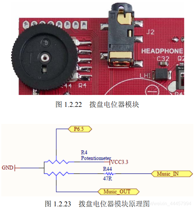
所用被测信号为配套实验板的拨盘电位器输出
信号引脚在0~3.3V之间可调。
测量引脚复用输入
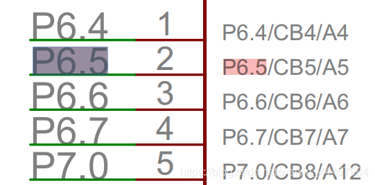
P6.5对应A5
将P6.5复用输入
    //P6.5 ADC option select
    GPIO_setAsPeripheralModuleFunctionInputPin(
            GPIO_PORT_P6,
            GPIO_PIN5
            );
配置ADC模块
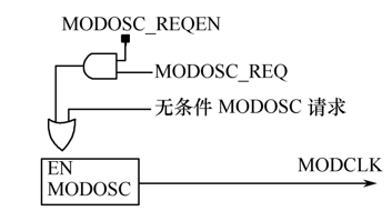
ADC模块时钟源选为MODOSC,不分频
内部模块振荡器(MODOSC)能够产生约4.8MHz的MODCLK时钟。Flash控制器模块、ADC_12模块等片内外设都可使用MODCLK作为内部参考时钟
    //Initialize the ADC12_A Module
    /*
     * Base address of ADC12_A Module
     * Use internal ADC12_A bit as sample/hold signal to start conversion
     * USE MODOSC 5MHZ Digital Oscillator as clock source
     * Use default clock divider of 1
     */
    ADC12_A_init(ADC12_A_BASE,
            ADC12_A_SAMPLEHOLDSOURCE_SC,
            ADC12_A_CLOCKSOURCE_ADC12OSC,
            ADC12_A_CLOCKDIVIDER_1);

	ADC12_A_enable(ADC12_A_BASE);
配置采样定时器
    /*
     * Base address of ADC12_A Module
     * For memory buffers 0-7 sample/hold for 64 clock cycles
     * For memory buffers 8-15 sample/hold for 4 clock cycles (default)
     * Disable Multiple Sampling
     */
    ADC12_A_setupSamplingTimer(ADC12_A_BASE,
            ADC12_A_CYCLEHOLD_64_CYCLES,
            ADC12_A_CYCLEHOLD_4_CYCLES,
            ADC12_A_MULTIPLESAMPLESDISABLE);
配置采样结果缓冲寄存器
选择输入信号为A5
正参考电压源选为AVcc
负参考电压源选为AVss
//Configure Memory Buffer
/*
* Base address of the ADC12_A Module
* Configure memory buffer 0
* Map input A5 to memory buffer 0
* Vref+ = AVcc
* Vr- = AVss
* Memory buffer 0 is not the end of a sequence
*/
ADC12_A_configureMemoryParam param = {0};
param.memoryBufferControlIndex = ADC12_A_MEMORY_0;
param.inputSourceSelect = ADC12_A_INPUT_A5;
param.positiveRefVoltageSourceSelect = ADC12_A_VREFPOS_AVCC;
param.negativeRefVoltageSourceSelect = ADC12_A_VREFNEG_AVSS;
param.endOfSequence = ADC12_A_NOTENDOFSEQUENCE;
ADC12_A_configureMemory(ADC12_A_BASE ,¶m);
配置ADC中断
因使用的是ADC12_A_MEMORY_0,故使能为Enable memory buffer 0 interrupt
    //Enable memory buffer 0 interrupt
    ADC12_A_clearInterrupt(ADC12_A_BASE,
            ADC12IFG0);
    ADC12_A_enableInterrupt(ADC12_A_BASE,
            ADC12IE0);
启动ADC转换
    while(1)
    {
        //Enable/Start sampling and conversion
        /*
         * Base address of ADC12_A Module
         * Start the conversion into memory buffer 0
         * Use the single-channel, single-conversion mode
         */
        ADC12_A_startConversion(ADC12_A_BASE, ADC12_A_MEMORY_0, ADC12_A_SINGLECHANNEL);

        //LPM0, ADC12_A_ISR will force exit
        __bis_SR_register(LPM0_bits + GIE);
        //for Debugger
        __no_operation();
    }
ADC中断服务函数
当被测电压大于0.5*AVcc时,点亮LED
反之熄灭LED,并打印所测电压值
case为ADC12_A_MEMORY_0对应的Vector 6
#pragma vector=ADC12_VECTOR
__interrupt
void ADC12_A_ISR (void)
{
    uint16_t Measured = 0;
    switch (__even_in_range(ADC12IV,34))
    {
        case  0: break;   //Vector  0:  No interrupt
        case  2: break;   //Vector  2:  ADC overflow
        case  4: break;   //Vector  4:  ADC timing overflow
        case  6:          //Vector  6:  ADC12IFG0
                 //Is Memory Buffer 0 = A5 > 0.5AVcc?
                 Measured = ADC12_A_getResults(ADC12_A_BASE, ADC12_A_MEMORY_0);
                 if (Measured >= 0x7ff)
                 {
                     //set P1.0
                     GPIO_setOutputHighOnPin(GPIO_PORT_P1, GPIO_PIN0);
                 }
                 else
                 {
                     //Clear P1.0 LED off
                     GPIO_setOutputLowOnPin(GPIO_PORT_P1, GPIO_PIN0);
                 }
                 UART_printf(USCI_A1_BASE, "Measured_Volt: %f\r\n", (float)Measured/0xfff*3.3);
                 //Exit active CPU
                 __bic_SR_register_on_exit(LPM0_bits);
        case  8: break;   //Vector  8:  ADC12IFG1
        case 10: break;   //Vector 10:  ADC12IFG2
        case 12: break;   //Vector 12:  ADC12IFG3
        case 14: break;   //Vector 14:  ADC12IFG4
        case 16: break;   //Vector 16:  ADC12IFG5
        case 18: break;   //Vector 18:  ADC12IFG6
        case 20: break;   //Vector 20:  ADC12IFG7
        case 22: break;   //Vector 22:  ADC12IFG8
        case 24: break;   //Vector 24:  ADC12IFG9
        case 26: break;   //Vector 26:  ADC12IFG10
        case 28: break;   //Vector 28:  ADC12IFG11
        case 30: break;   //Vector 30:  ADC12IFG12
        case 32: break;   //Vector 32:  ADC12IFG13
        case 34: break;   //Vector 34:  ADC12IFG14
        default: break;
    }
}
整体代码
#include "driverlib.h"
#define MCLK_IN_HZ 25000000
#define delay_us(x) __delay_cycles((MCLK_IN_HZ/1000000*(x)))
#define delay_ms(x) __delay_cycles((MCLK_IN_HZ/1000*(x)))
void UART_printf(uint16_t baseAddress, const char *format,...);
bool UART_Init(uint16_t baseAddress, uint32_t Baudrate);
void SystemClock_Init(void)
{
PMM_setVCore(PMM_CORE_LEVEL_3); //高主频工作需要较高的核心电压
//XT1引脚复用
GPIO_setAsPeripheralModuleFunctionInputPin(GPIO_PORT_P5, GPIO_PIN4);
GPIO_setAsPeripheralModuleFunctionOutputPin(GPIO_PORT_P5, GPIO_PIN5);
//起振XT1
UCS_turnOnLFXT1(UCS_XT1_DRIVE_3,UCS_XCAP_3);
//XT2引脚复用
GPIO_setAsPeripheralModuleFunctionInputPin(GPIO_PORT_P5, GPIO_PIN2);
GPIO_setAsPeripheralModuleFunctionOutputPin(GPIO_PORT_P5, GPIO_PIN3);
//起振XT2
UCS_turnOnXT2(UCS_XT2_DRIVE_4MHZ_8MHZ);
//XT2作为FLL参考时钟,先8分频,再50倍频 4MHz / 8 * 50 = 25MHz
UCS_initClockSignal(UCS_FLLREF, UCS_XT2CLK_SELECT, UCS_CLOCK_DIVIDER_8);
UCS_initFLLSettle(25000, 50);
//XT1作为ACLK时钟源 = 32768Hz
UCS_initClockSignal(UCS_ACLK, UCS_XT1CLK_SELECT, UCS_CLOCK_DIVIDER_1);
//DCOCLK作为MCLK时钟源 = 25MHz
UCS_initClockSignal(UCS_MCLK, UCS_DCOCLK_SELECT, UCS_CLOCK_DIVIDER_1);
//DCOCLK作为SMCLK时钟源 = 25MHz
UCS_initClockSignal(UCS_SMCLK, UCS_DCOCLK_SELECT, UCS_CLOCK_DIVIDER_1);
//设置外部时钟源的频率,使得在调用UCS_getMCLK, UCS_getSMCLK 或 UCS_getACLK时可得到正确值
UCS_setExternalClockSource(32768, 4000000);
}
void ADC_Test_Init(void)
{
//P6.5 ADC option select
GPIO_setAsPeripheralModuleFunctionInputPin(
GPIO_PORT_P6,
GPIO_PIN5
);
//Initialize the ADC12_A Module
/*
* Base address of ADC12_A Module
* Use internal ADC12_A bit as sample/hold signal to start conversion
* USE MODOSC 5MHZ Digital Oscillator as clock source
* Use default clock divider of 1
*/
ADC12_A_init(ADC12_A_BASE,
ADC12_A_SAMPLEHOLDSOURCE_SC,
ADC12_A_CLOCKSOURCE_ADC12OSC,
ADC12_A_CLOCKDIVIDER_1);
ADC12_A_enable(ADC12_A_BASE);
/*
* Base address of ADC12_A Module
* For memory buffers 0-7 sample/hold for 64 clock cycles
* For memory buffers 8-15 sample/hold for 4 clock cycles (default)
* Disable Multiple Sampling
*/
ADC12_A_setupSamplingTimer(ADC12_A_BASE,
ADC12_A_CYCLEHOLD_64_CYCLES,
ADC12_A_CYCLEHOLD_4_CYCLES,
ADC12_A_MULTIPLESAMPLESDISABLE);
//Configure Memory Buffer
/*
* Base address of the ADC12_A Module
* Configure memory buffer 0
* Map input A5 to memory buffer 0
* Vref+ = AVcc
* Vr- = AVss
* Memory buffer 0 is not the end of a sequence
*/
ADC12_A_configureMemoryParam param = {0};
param.memoryBufferControlIndex = ADC12_A_MEMORY_0;
param.inputSourceSelect = ADC12_A_INPUT_A5;
param.positiveRefVoltageSourceSelect = ADC12_A_VREFPOS_AVCC;
param.negativeRefVoltageSourceSelect = ADC12_A_VREFNEG_AVSS;
param.endOfSequence = ADC12_A_NOTENDOFSEQUENCE;
ADC12_A_configureMemory(ADC12_A_BASE ,¶m);
//Enable memory buffer 0 interrupt
ADC12_A_clearInterrupt(ADC12_A_BASE,
ADC12IFG0);
ADC12_A_enableInterrupt(ADC12_A_BASE,
ADC12IE0);
}
int main(void)
{
WDT_A_hold(WDT_A_BASE);
SystemClock_Init();
UART_Init(USCI_A1_BASE, 115200);
ADC_Test_Init();
GPIO_setAsOutputPin(GPIO_PORT_P1, GPIO_PIN0);
while(1)
{
//Enable/Start sampling and conversion
/*
* Base address of ADC12_A Module
* Start the conversion into memory buffer 0
* Use the single-channel, single-conversion mode
*/
ADC12_A_startConversion(ADC12_A_BASE, ADC12_A_MEMORY_0, ADC12_A_SINGLECHANNEL);
//LPM0, ADC12_A_ISR will force exit
__bis_SR_register(LPM0_bits + GIE);
//for Debugger
__no_operation();
}
}
#pragma vector=ADC12_VECTOR
__interrupt
void ADC12_A_ISR (void)
{
uint16_t Measured = 0;
switch (__even_in_range(ADC12IV,34))
{
case 0: break; //Vector 0: No interrupt
case 2: break; //Vector 2: ADC overflow
case 4: break; //Vector 4: ADC timing overflow
case 6: //Vector 6: ADC12IFG0
//Is Memory Buffer 0 = A5 > 0.5AVcc?
Measured = ADC12_A_getResults(ADC12_A_BASE, ADC12_A_MEMORY_0);
if (Measured >= 0x7ff)
{
//set P1.0
GPIO_setOutputHighOnPin(GPIO_PORT_P1, GPIO_PIN0);
}
else
{
//Clear P1.0 LED off
GPIO_setOutputLowOnPin(GPIO_PORT_P1, GPIO_PIN0);
}
UART_printf(USCI_A1_BASE, "Measured_Volt: %f\r\n", (float)Measured/0xfff*3.3);
//Exit active CPU
__bic_SR_register_on_exit(LPM0_bits);
case 8: break; //Vector 8: ADC12IFG1
case 10: break; //Vector 10: ADC12IFG2
case 12: break; //Vector 12: ADC12IFG3
case 14: break; //Vector 14: ADC12IFG4
case 16: break; //Vector 16: ADC12IFG5
case 18: break; //Vector 18: ADC12IFG6
case 20: break; //Vector 20: ADC12IFG7
case 22: break; //Vector 22: ADC12IFG8
case 24: break; //Vector 24: ADC12IFG9
case 26: break; //Vector 26: ADC12IFG10
case 28: break; //Vector 28: ADC12IFG11
case 30: break; //Vector 30: ADC12IFG12
case 32: break; //Vector 32: ADC12IFG13
case 34: break; //Vector 34: ADC12IFG14
default: break;
}
}
#include <string.h>
#include <stdarg.h>
#include <stdio.h>
void UART_printf(uint16_t baseAddress, const char *format,...)
{
uint32_t length;
va_list args;
uint32_t i;
char TxBuffer[128] = {0};
va_start(args, format);
length = vsnprintf((char*)TxBuffer, sizeof(TxBuffer)+1, (char*)format, args);
va_end(args);
for(i = 0; i < length; i++)
USCI_A_UART_transmitData(baseAddress, TxBuffer[i]);
}
bool UART_Init(uint16_t baseAddress, uint32_t Baudrate)
{
float UART_Temp = 0;
USCI_A_UART_initParam huart = {0};
if(baseAddress == USCI_A0_BASE) //P3.3, P3.4 = USCI_A0 TXD/RXD
{
GPIO_setAsPeripheralModuleFunctionOutputPin(GPIO_PORT_P3, GPIO_PIN3);
GPIO_setAsPeripheralModuleFunctionInputPin(GPIO_PORT_P3, GPIO_PIN4);
}
else if(baseAddress == USCI_A1_BASE) //P4.4, P4.5 = USCI_A1 TXD/RXD
{
GPIO_setAsPeripheralModuleFunctionOutputPin(GPIO_PORT_P4, GPIO_PIN4);
GPIO_setAsPeripheralModuleFunctionInputPin(GPIO_PORT_P4, GPIO_PIN5);
}
if(Baudrate <= 9600)
{
huart.selectClockSource = USCI_A_UART_CLOCKSOURCE_ACLK;
UART_Temp = (float)UCS_getACLK()/Baudrate;
}
else
{
huart.selectClockSource = USCI_A_UART_CLOCKSOURCE_SMCLK;
UART_Temp = (float)UCS_getSMCLK()/Baudrate;
}
if(UART_Temp < 16)
huart.overSampling = USCI_A_UART_LOW_FREQUENCY_BAUDRATE_GENERATION;
else
{
huart.overSampling = USCI_A_UART_OVERSAMPLING_BAUDRATE_GENERATION;
UART_Temp /= 16;
}
huart.clockPrescalar = (int)UART_Temp;
if(huart.overSampling == USCI_A_UART_LOW_FREQUENCY_BAUDRATE_GENERATION)
{
huart.secondModReg = (int)((UART_Temp - huart.clockPrescalar) * 8);
}
else
{
huart.firstModReg = (int)((UART_Temp - huart.clockPrescalar) * 16);
}
huart.parity = USCI_A_UART_NO_PARITY;
huart.msborLsbFirst = USCI_A_UART_LSB_FIRST;
huart.numberofStopBits = USCI_A_UART_ONE_STOP_BIT;
huart.uartMode = USCI_A_UART_MODE;
if (STATUS_FAIL == USCI_A_UART_init(baseAddress, &huart))
{
return STATUS_FAIL;
}
//Enable UART module for operation
USCI_A_UART_enable(baseAddress);
//Enable Receive Interrupt
USCI_A_UART_clearInterrupt(baseAddress, USCI_A_UART_RECEIVE_INTERRUPT);
USCI_A_UART_enableInterrupt(baseAddress, USCI_A_UART_RECEIVE_INTERRUPT);
return STATUS_SUCCESS;
}
//******************************************************************************
//
//This is the USCI_A0 interrupt vector service routine.
//
//******************************************************************************
#pragma vector=USCI_A0_VECTOR
__interrupt void USCI_A0_ISR (void)
{
uint8_t receivedData = 0;
switch (__even_in_range(UCA0IV,4))
{
//Vector 2 - RXIFG
case 2:
receivedData = USCI_A_UART_receiveData(USCI_A0_BASE);
USCI_A_UART_transmitData(USCI_A0_BASE,receivedData);
break;
default:
break;
}
}
//******************************************************************************
//
//This is the USCI_A1 interrupt vector service routine.
//
//******************************************************************************
#pragma vector=USCI_A1_VECTOR
__interrupt void USCI_A1_ISR (void)
{
uint8_t receivedData = 0;
switch (__even_in_range(UCA1IV,4))
{
//Vector 2 - RXIFG
case 2:
receivedData = USCI_A_UART_receiveData(USCI_A1_BASE);
USCI_A_UART_transmitData(USCI_A1_BASE,receivedData);
break;
default:
break;
}
}
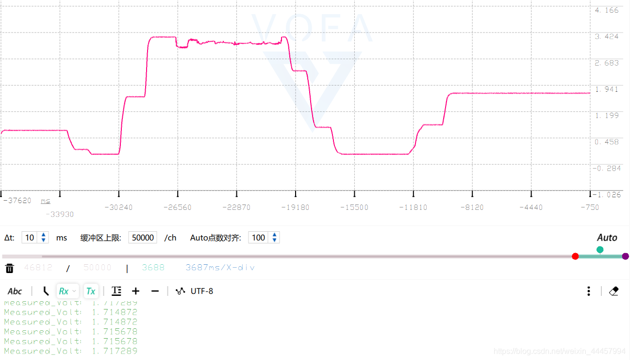
实验结果
连上串口,转动电位器,得到被测信号波形:
采用内部参考电压的单通道采样
(改自官方例程)
测量引脚复用输入
    //P6.5 ADC option select
    GPIO_setAsPeripheralModuleFunctionInputPin(GPIO_PORT_P6, GPIO_PIN5);
配置ADC模块
正参考电压源选为内部参考电压,其他部分同上一个实验
//Initialize the ADC12_A Module
/*
* Base address of ADC12_A Module
* Use internal ADC12_A bit as sample/hold signal to start conversion
* USE MODOSC 5MHZ Digital Oscillator as clock source
* Use default clock divider of 1
*/
ADC12_A_init(ADC12_A_BASE,
ADC12_A_SAMPLEHOLDSOURCE_SC,
ADC12_A_CLOCKSOURCE_ADC12OSC,
ADC12_A_CLOCKDIVIDER_1);
ADC12_A_enable(ADC12_A_BASE);
/*
* Base address of ADC12_A Module
* For memory buffers 0-7 sample/hold for 64 clock cycles
* For memory buffers 8-15 sample/hold for 4 clock cycles (default)
* Disable Multiple Sampling
*/
ADC12_A_setupSamplingTimer(ADC12_A_BASE,
ADC12_A_CYCLEHOLD_64_CYCLES,
ADC12_A_CYCLEHOLD_4_CYCLES,
ADC12_A_MULTIPLESAMPLESDISABLE);
//Configure Memory Buffer
/*
* Base address of the ADC12_A Module
* Configure memory buffer 0
* Map input A0 to memory buffer 0
* Vr+ = Vref+ (int)
* Vr- = AVss
* Memory buffer 0 is not the end of a sequence
*/
ADC12_A_configureMemoryParam param = {0};
param.memoryBufferControlIndex = ADC12_A_MEMORY_0;
param.inputSourceSelect = ADC12_A_INPUT_A5;
param.positiveRefVoltageSourceSelect = ADC12_A_VREFPOS_INT;
param.negativeRefVoltageSourceSelect = ADC12_A_VREFNEG_AVSS;
param.endOfSequence = ADC12_A_NOTENDOFSEQUENCE;
ADC12_A_configureMemory(ADC12_A_BASE ,¶m);
配置内部参考电压
     //Configure internal reference
     //If ref generator busy, WAIT
     while ( REF_ACTIVE == Ref_isRefGenBusy(REF_BASE) ) ;
     //Select internal ref = 1.5V
     Ref_setReferenceVoltage(REF_BASE,
         REF_VREF1_5V);
     //Internal Reference ON
     Ref_enableReferenceVoltage(REF_BASE);

     //Delay (~75us) for Ref to settle
     delay_us(75);
其中内部参考电压可设为1.5V、2V、2.5V
//*****************************************************************************
//
// The following are values that can be passed to the referenceVoltageSelect
// parameter for functions: Ref_setReferenceVoltage().
//
//*****************************************************************************
#define REF_VREF1_5V                                                (REFVSEL_0)
#define REF_VREF2_0V                                                (REFVSEL_1)
#define REF_VREF2_5V                                                (REFVSEL_2)
启动转换并将结果由串口发送
    while(1)
    {
        //Enable/Start first sampling and conversion cycle
        /*
         * Base address of ADC12_A Module
         * Start the conversion into memory buffer 0
         * Use the single-channel, single-conversion mode
         */
        ADC12_A_startConversion(ADC12_A_BASE, ADC12_A_MEMORY_0, ADC12_A_SINGLECHANNEL);

        //Poll for interrupt on memory buffer 0
        while (!ADC12_A_getInterruptStatus(ADC12_A_BASE, ADC12IFG0));

        Measured = ADC12_A_getResults(ADC12_A_BASE, ADC12_A_MEMORY_0);

        UART_printf(USCI_A1_BASE, "Measured_Volt: %f\r\n", (float)Measured/0xfff*1.5);

        //SET BREAKPOINT HERE
        __no_operation();
    }
整体代码
#include "driverlib.h"
#define MCLK_IN_HZ 25000000
#define delay_us(x) __delay_cycles((MCLK_IN_HZ/1000000*(x)))
#define delay_ms(x) __delay_cycles((MCLK_IN_HZ/1000*(x)))
void UART_printf(uint16_t baseAddress, const char *format,...);
bool UART_Init(uint16_t baseAddress, uint32_t Baudrate);
void SystemClock_Init(void)
{
PMM_setVCore(PMM_CORE_LEVEL_3); //高主频工作需要较高的核心电压
//XT1引脚复用
GPIO_setAsPeripheralModuleFunctionInputPin(GPIO_PORT_P5, GPIO_PIN4);
GPIO_setAsPeripheralModuleFunctionOutputPin(GPIO_PORT_P5, GPIO_PIN5);
//起振XT1
UCS_turnOnLFXT1(UCS_XT1_DRIVE_3,UCS_XCAP_3);
//XT2引脚复用
GPIO_setAsPeripheralModuleFunctionInputPin(GPIO_PORT_P5, GPIO_PIN2);
GPIO_setAsPeripheralModuleFunctionOutputPin(GPIO_PORT_P5, GPIO_PIN3);
//起振XT2
UCS_turnOnXT2(UCS_XT2_DRIVE_4MHZ_8MHZ);
//XT2作为FLL参考时钟,先8分频,再50倍频 4MHz / 8 * 50 = 25MHz
UCS_initClockSignal(UCS_FLLREF, UCS_XT2CLK_SELECT, UCS_CLOCK_DIVIDER_8);
UCS_initFLLSettle(25000, 50);
//XT1作为ACLK时钟源 = 32768Hz
UCS_initClockSignal(UCS_ACLK, UCS_XT1CLK_SELECT, UCS_CLOCK_DIVIDER_1);
//DCOCLK作为MCLK时钟源 = 25MHz
UCS_initClockSignal(UCS_MCLK, UCS_DCOCLK_SELECT, UCS_CLOCK_DIVIDER_1);
//DCOCLK作为SMCLK时钟源 = 25MHz
UCS_initClockSignal(UCS_SMCLK, UCS_DCOCLK_SELECT, UCS_CLOCK_DIVIDER_1);
//设置外部时钟源的频率,使得在调用UCS_getMCLK, UCS_getSMCLK 或 UCS_getACLK时可得到正确值
UCS_setExternalClockSource(32768, 4000000);
}
void ADC_Test_Init(void)
{
//P6.5 ADC option select
GPIO_setAsPeripheralModuleFunctionInputPin(GPIO_PORT_P6, GPIO_PIN5);
//Initialize the ADC12_A Module
/*
* Base address of ADC12_A Module
* Use internal ADC12_A bit as sample/hold signal to start conversion
* USE MODOSC 5MHZ Digital Oscillator as clock source
* Use default clock divider of 1
*/
ADC12_A_init(ADC12_A_BASE,
ADC12_A_SAMPLEHOLDSOURCE_SC,
ADC12_A_CLOCKSOURCE_ADC12OSC,
ADC12_A_CLOCKDIVIDER_1);
ADC12_A_enable(ADC12_A_BASE);
/*
* Base address of ADC12_A Module
* For memory buffers 0-7 sample/hold for 64 clock cycles
* For memory buffers 8-15 sample/hold for 4 clock cycles (default)
* Disable Multiple Sampling
*/
ADC12_A_setupSamplingTimer(ADC12_A_BASE,
ADC12_A_CYCLEHOLD_64_CYCLES,
ADC12_A_CYCLEHOLD_4_CYCLES,
ADC12_A_MULTIPLESAMPLESDISABLE);
//Configure Memory Buffer
/*
* Base address of the ADC12_A Module
* Configure memory buffer 0
* Map input A0 to memory buffer 0
* Vr+ = Vref+ (int)
* Vr- = AVss
* Memory buffer 0 is not the end of a sequence
*/
ADC12_A_configureMemoryParam param = {0};
param.memoryBufferControlIndex = ADC12_A_MEMORY_0;
param.inputSourceSelect = ADC12_A_INPUT_A5;
param.positiveRefVoltageSourceSelect = ADC12_A_VREFPOS_INT;
param.negativeRefVoltageSourceSelect = ADC12_A_VREFNEG_AVSS;
param.endOfSequence = ADC12_A_NOTENDOFSEQUENCE;
ADC12_A_configureMemory(ADC12_A_BASE ,¶m);
//Configure internal reference
//If ref generator busy, WAIT
while ( REF_ACTIVE == Ref_isRefGenBusy(REF_BASE) ) ;
//Select internal ref = 1.5V
Ref_setReferenceVoltage(REF_BASE,
REF_VREF1_5V);
//Internal Reference ON
Ref_enableReferenceVoltage(REF_BASE);
//Delay (~75us) for Ref to settle
delay_us(75);
}
int main(void)
{
uint16_t Measured = 0;
WDT_A_hold(WDT_A_BASE);
SystemClock_Init();
UART_Init(USCI_A1_BASE, 115200);
ADC_Test_Init();
while(1)
{
//Enable/Start first sampling and conversion cycle
/*
* Base address of ADC12_A Module
* Start the conversion into memory buffer 0
* Use the single-channel, single-conversion mode
*/
ADC12_A_startConversion(ADC12_A_BASE, ADC12_A_MEMORY_0, ADC12_A_SINGLECHANNEL);
//Poll for interrupt on memory buffer 0
while (!ADC12_A_getInterruptStatus(ADC12_A_BASE, ADC12IFG0));
Measured = ADC12_A_getResults(ADC12_A_BASE, ADC12_A_MEMORY_0);
UART_printf(USCI_A1_BASE, "Measured_Volt: %f\r\n", (float)Measured/0xfff*1.5);
//SET BREAKPOINT HERE
__no_operation();
}
}
#include <string.h>
#include <stdarg.h>
#include <stdio.h>
void UART_printf(uint16_t baseAddress, const char *format,...)
{
uint32_t length;
va_list args;
uint32_t i;
char TxBuffer[128] = {0};
va_start(args, format);
length = vsnprintf((char*)TxBuffer, sizeof(TxBuffer)+1, (char*)format, args);
va_end(args);
for(i = 0; i < length; i++)
USCI_A_UART_transmitData(baseAddress, TxBuffer[i]);
}
bool UART_Init(uint16_t baseAddress, uint32_t Baudrate)
{
float UART_Temp = 0;
USCI_A_UART_initParam huart = {0};
if(baseAddress == USCI_A0_BASE) //P3.3, P3.4 = USCI_A0 TXD/RXD
{
GPIO_setAsPeripheralModuleFunctionOutputPin(GPIO_PORT_P3, GPIO_PIN3);
GPIO_setAsPeripheralModuleFunctionInputPin(GPIO_PORT_P3, GPIO_PIN4);
}
else if(baseAddress == USCI_A1_BASE) //P4.4, P4.5 = USCI_A1 TXD/RXD
{
GPIO_setAsPeripheralModuleFunctionOutputPin(GPIO_PORT_P4, GPIO_PIN4);
GPIO_setAsPeripheralModuleFunctionInputPin(GPIO_PORT_P4, GPIO_PIN5);
}
if(Baudrate <= 9600)
{
huart.selectClockSource = USCI_A_UART_CLOCKSOURCE_ACLK;
UART_Temp = (float)UCS_getACLK()/Baudrate;
}
else
{
huart.selectClockSource = USCI_A_UART_CLOCKSOURCE_SMCLK;
UART_Temp = (float)UCS_getSMCLK()/Baudrate;
}
if(UART_Temp < 16)
huart.overSampling = USCI_A_UART_LOW_FREQUENCY_BAUDRATE_GENERATION;
else
{
huart.overSampling = USCI_A_UART_OVERSAMPLING_BAUDRATE_GENERATION;
UART_Temp /= 16;
}
huart.clockPrescalar = (int)UART_Temp;
if(huart.overSampling == USCI_A_UART_LOW_FREQUENCY_BAUDRATE_GENERATION)
{
huart.secondModReg = (int)((UART_Temp - huart.clockPrescalar) * 8);
}
else
{
huart.firstModReg = (int)((UART_Temp - huart.clockPrescalar) * 16);
}
huart.parity = USCI_A_UART_NO_PARITY;
huart.msborLsbFirst = USCI_A_UART_LSB_FIRST;
huart.numberofStopBits = USCI_A_UART_ONE_STOP_BIT;
huart.uartMode = USCI_A_UART_MODE;
if (STATUS_FAIL == USCI_A_UART_init(baseAddress, &huart))
{
return STATUS_FAIL;
}
//Enable UART module for operation
USCI_A_UART_enable(baseAddress);
//Enable Receive Interrupt
USCI_A_UART_clearInterrupt(baseAddress, USCI_A_UART_RECEIVE_INTERRUPT);
USCI_A_UART_enableInterrupt(baseAddress, USCI_A_UART_RECEIVE_INTERRUPT);
return STATUS_SUCCESS;
}
//******************************************************************************
//
//This is the USCI_A0 interrupt vector service routine.
//
//******************************************************************************
#pragma vector=USCI_A0_VECTOR
__interrupt void USCI_A0_ISR (void)
{
uint8_t receivedData = 0;
switch (__even_in_range(UCA0IV,4))
{
//Vector 2 - RXIFG
case 2:
receivedData = USCI_A_UART_receiveData(USCI_A0_BASE);
USCI_A_UART_transmitData(USCI_A0_BASE,receivedData);
break;
default:
break;
}
}
//******************************************************************************
//
//This is the USCI_A1 interrupt vector service routine.
//
//******************************************************************************
#pragma vector=USCI_A1_VECTOR
__interrupt void USCI_A1_ISR (void)
{
uint8_t receivedData = 0;
switch (__even_in_range(UCA1IV,4))
{
//Vector 2 - RXIFG
case 2:
receivedData = USCI_A_UART_receiveData(USCI_A1_BASE);
USCI_A_UART_transmitData(USCI_A1_BASE,receivedData);
break;
default:
break;
}
}
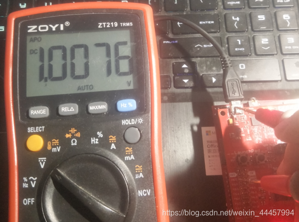
实验结果
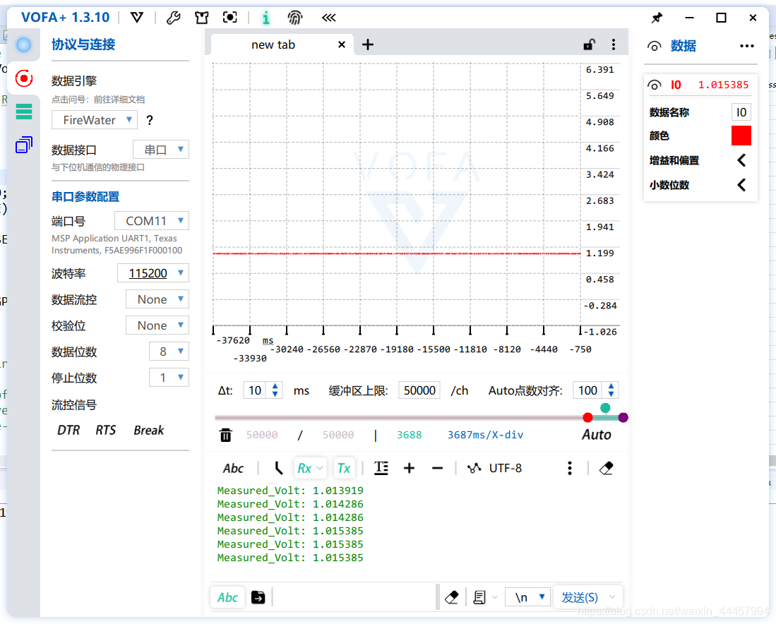
万用表测得此时P6.5电压为1.0076V
参考电压为1.5V时
串口打印电压为1.015385V,误差0.77%
(使用中断)序列多通道转换
(改自官方例程)
测量引脚复用输入
由于开发板上只有一个电位器,故将电位器所连的P6.5通过杜邦线再连至P6.4
P6.4、P6.5复用输入
    //Enable A/D channel inputs
    GPIO_setAsPeripheralModuleFunctionInputPin(GPIO_PORT_P6,
        GPIO_PIN4 | GPIO_PIN5
        );
配置ADC模块
使能多通道采样
    //Initialize the ADC12_A Module
    /*
     * Base address of ADC12_A Module
     * Use internal ADC12_A bit as sample/hold signal to start conversion
     * USE MODOSC 5MHZ Digital Oscillator as clock source
     * Use default clock divider of 1
     */
    ADC12_A_init(ADC12_A_BASE,
        ADC12_A_SAMPLEHOLDSOURCE_SC,
        ADC12_A_CLOCKSOURCE_ADC12OSC,
        ADC12_A_CLOCKDIVIDER_1
        );

    ADC12_A_enable(ADC12_A_BASE);

    /*
     * Base address of ADC12_A Module
     * For memory buffers 0-7 sample/hold for 256 clock cycles
     * For memory buffers 8-15 sample/hold for 4 clock cycles (default)
     * Enable Multiple Sampling
     */
    ADC12_A_setupSamplingTimer(ADC12_A_BASE,
        ADC12_A_CYCLEHOLD_128_CYCLES,
        ADC12_A_CYCLEHOLD_4_CYCLES,
        ADC12_A_MULTIPLESAMPLESENABLE);
配置采样存储器
正参考电压都设为AVcc
负参考电压都设为AVss
其中A4不是序列的结尾
A5是序列的结尾
ADC12_A_configureMemoryParam param = {0};
param.positiveRefVoltageSourceSelect = ADC12_A_VREFPOS_AVCC;
param.negativeRefVoltageSourceSelect = ADC12_A_VREFNEG_AVSS;
//Configure Memory Buffers
/*
* Base address of the ADC12_A Module
* Configure memory buffer 4
* Map input A4 to memory buffer 4
* Vref+ = AVcc
* Vref- = AVss
* Memory buffer 4 is not the end of a sequence
*/
param.memoryBufferControlIndex = ADC12_A_MEMORY_4;
param.inputSourceSelect = ADC12_A_INPUT_A4;
param.endOfSequence = ADC12_A_NOTENDOFSEQUENCE;
ADC12_A_configureMemory(ADC12_A_BASE ,¶m);
/*
* Base address of the ADC12_A Module
* Configure memory buffer 5
* Map input A5 to memory buffer 5
* Vr+ = AVcc
* Vr- = AVss
* Memory buffer 5 IS the end of a sequence
*/
param.memoryBufferControlIndex = ADC12_A_MEMORY_5;
param.inputSourceSelect = ADC12_A_INPUT_A5;
param.endOfSequence = ADC12_A_ENDOFSEQUENCE;
ADC12_A_configureMemory(ADC12_A_BASE ,¶m);
配置ADC中断
当序列转换结束,进入中断,故设为5的中断
    //Enable memory buffer 5 interrupt
    ADC12_A_clearInterrupt(ADC12_A_BASE, ADC12IFG5);
    ADC12_A_enableInterrupt(ADC12_A_BASE, ADC12IE5);
开始ADC采样
开始转换序列,起始为通道4
模式为序列通道多次转换
    //Enable/Start first sampling and conversion cycle
    /*
     * Base address of ADC12_A Module
     * Start the conversion into memory buffer 0
     * Use the repeated sequence of channels
     */
    ADC12_A_startConversion(ADC12_A_BASE, ADC12_A_MEMORY_4, ADC12_A_REPEATED_SEQOFCHANNELS);
配置ADC中断服务函数
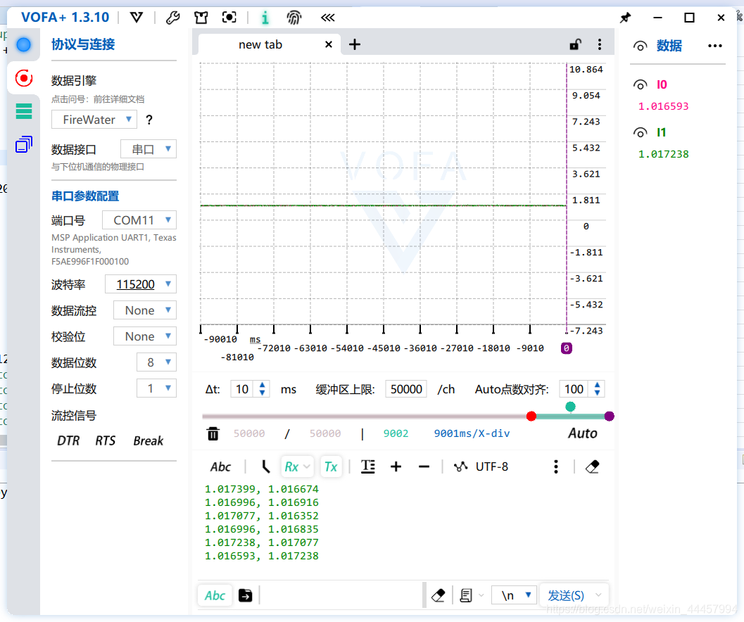
序列转换结束进入一次中断,每累计转换Num_of_Results次,打印一次电压平均值。
#pragma vector=ADC12_VECTOR
__interrupt
void ADC12ISR (void)
{
    static uint16_t index = 0;

    switch (__even_in_range(ADC12IV,34)){
        case  0: break;   //Vector  0:  No interrupt
        case  2: break;   //Vector  2:  ADC overflow
        case  4: break;   //Vector  4:  ADC timing overflow
        case  6: break;   //Vector  6:  ADC12IFG0
        case  8: break;   //Vector  8:  ADC12IFG1
        case 10: break;   //Vector 10:  ADC12IFG2
        case 12: break;   //Vector 12:  ADC12IFG3
        case 14: break;   //Vector 14:  ADC12IFG4
        case 16:          //Vector 16:  ADC12IFG5
            //Move A4 results, IFG is cleared
            A4results[index] = ADC12_A_getResults(ADC12_A_BASE, ADC12_A_MEMORY_4);
            //Move A5 results, IFG is cleared
            A5results[index] = ADC12_A_getResults(ADC12_A_BASE, ADC12_A_MEMORY_5);

            //Increment results index, modulo; Set BREAKPOINT here
            index++;

            if (index == Num_of_Results)
            {
                float A4_Volt, A5_Volt;
                uint8_t i = 0;
                index = 0;
                for(i = 0, A4_Volt = 0; i < Num_of_Results; i++)
                    A4_Volt += A4results[i];
                A4_Volt = A4_Volt/10/0xfff*3.3;
                for(i = 0, A5_Volt = 0; i < Num_of_Results; i++)
                    A5_Volt += A5results[i];
                A5_Volt = A5_Volt/10/0xfff*3.3;
                UART_printf(USCI_A1_BASE, "%f %f\r\n", A4_Volt, A5_Volt);
            }
            break;
        case 18: break;   //Vector 18:  ADC12IFG6
        case 20: break;   //Vector 20:  ADC12IFG7
        case 22: break;   //Vector 22:  ADC12IFG8
        case 24: break;   //Vector 24:  ADC12IFG9
        case 26: break;   //Vector 26:  ADC12IFG10
        case 28: break;   //Vector 28:  ADC12IFG11
        case 30: break;   //Vector 30:  ADC12IFG12
        case 32: break;   //Vector 32:  ADC12IFG13
        case 34: break;   //Vector 34:  ADC12IFG14
        default: break;
    }
}
整体代码
#include "driverlib.h"
#define MCLK_IN_HZ 25000000
#define delay_us(x) __delay_cycles((MCLK_IN_HZ/1000000*(x)))
#define delay_ms(x) __delay_cycles((MCLK_IN_HZ/1000*(x)))
void UART_printf(uint16_t baseAddress, const char *format,...);
bool UART_Init(uint16_t baseAddress, uint32_t Baudrate);
void SystemClock_Init(void)
{
PMM_setVCore(PMM_CORE_LEVEL_3); //高主频工作需要较高的核心电压
//XT1引脚复用
GPIO_setAsPeripheralModuleFunctionInputPin(GPIO_PORT_P5, GPIO_PIN4);
GPIO_setAsPeripheralModuleFunctionOutputPin(GPIO_PORT_P5, GPIO_PIN5);
//起振XT1
UCS_turnOnLFXT1(UCS_XT1_DRIVE_3,UCS_XCAP_3);
//XT2引脚复用
GPIO_setAsPeripheralModuleFunctionInputPin(GPIO_PORT_P5, GPIO_PIN2);
GPIO_setAsPeripheralModuleFunctionOutputPin(GPIO_PORT_P5, GPIO_PIN3);
//起振XT2
UCS_turnOnXT2(UCS_XT2_DRIVE_4MHZ_8MHZ);
//XT2作为FLL参考时钟,先8分频,再50倍频 4MHz / 8 * 50 = 25MHz
UCS_initClockSignal(UCS_FLLREF, UCS_XT2CLK_SELECT, UCS_CLOCK_DIVIDER_8);
UCS_initFLLSettle(25000, 50);
//XT1作为ACLK时钟源 = 32768Hz
UCS_initClockSignal(UCS_ACLK, UCS_XT1CLK_SELECT, UCS_CLOCK_DIVIDER_1);
//DCOCLK作为MCLK时钟源 = 25MHz
UCS_initClockSignal(UCS_MCLK, UCS_DCOCLK_SELECT, UCS_CLOCK_DIVIDER_1);
//DCOCLK作为SMCLK时钟源 = 25MHz
UCS_initClockSignal(UCS_SMCLK, UCS_DCOCLK_SELECT, UCS_CLOCK_DIVIDER_1);
//设置外部时钟源的频率,使得在调用UCS_getMCLK, UCS_getSMCLK 或 UCS_getACLK时可得到正确值
UCS_setExternalClockSource(32768, 4000000);
}
#define Num_of_Results 10
volatile uint16_t A4results[Num_of_Results];
volatile uint16_t A5results[Num_of_Results];
void ADC_Test_Init(void)
{
//Enable A/D channel inputs
GPIO_setAsPeripheralModuleFunctionInputPin(GPIO_PORT_P6,
GPIO_PIN4 | GPIO_PIN5
);
//Initialize the ADC12_A Module
/*
* Base address of ADC12_A Module
* Use internal ADC12_A bit as sample/hold signal to start conversion
* USE MODOSC 5MHZ Digital Oscillator as clock source
* Use default clock divider of 1
*/
ADC12_A_init(ADC12_A_BASE,
ADC12_A_SAMPLEHOLDSOURCE_SC,
ADC12_A_CLOCKSOURCE_ADC12OSC,
ADC12_A_CLOCKDIVIDER_1
);
ADC12_A_enable(ADC12_A_BASE);
/*
* Base address of ADC12_A Module
* For memory buffers 0-7 sample/hold for 256 clock cycles
* For memory buffers 8-15 sample/hold for 4 clock cycles (default)
* Enable Multiple Sampling
*/
ADC12_A_setupSamplingTimer(ADC12_A_BASE,
ADC12_A_CYCLEHOLD_128_CYCLES,
ADC12_A_CYCLEHOLD_4_CYCLES,
ADC12_A_MULTIPLESAMPLESENABLE);
ADC12_A_configureMemoryParam param = {0};
param.positiveRefVoltageSourceSelect = ADC12_A_VREFPOS_AVCC;
param.negativeRefVoltageSourceSelect = ADC12_A_VREFNEG_AVSS;
//Configure Memory Buffers
/*
* Base address of the ADC12_A Module
* Configure memory buffer 4
* Map input A4 to memory buffer 4
* Vref+ = AVcc
* Vref- = AVss
* Memory buffer 4 is not the end of a sequence
*/
param.memoryBufferControlIndex = ADC12_A_MEMORY_4;
param.inputSourceSelect = ADC12_A_INPUT_A4;
param.endOfSequence = ADC12_A_NOTENDOFSEQUENCE;
ADC12_A_configureMemory(ADC12_A_BASE ,¶m);
/*
* Base address of the ADC12_A Module
* Configure memory buffer 5
* Map input A5 to memory buffer 5
* Vr+ = AVcc
* Vr- = AVss
* Memory buffer 5 IS the end of a sequence
*/
param.memoryBufferControlIndex = ADC12_A_MEMORY_5;
param.inputSourceSelect = ADC12_A_INPUT_A5;
param.endOfSequence = ADC12_A_ENDOFSEQUENCE;
ADC12_A_configureMemory(ADC12_A_BASE ,¶m);
//Enable memory buffer 5 interrupt
ADC12_A_clearInterrupt(ADC12_A_BASE, ADC12IFG5);
ADC12_A_enableInterrupt(ADC12_A_BASE, ADC12IE5);
//Enable/Start first sampling and conversion cycle
/*
* Base address of ADC12_A Module
* Start the conversion into memory buffer 0
* Use the repeated sequence of channels
*/
ADC12_A_startConversion(ADC12_A_BASE, ADC12_A_MEMORY_4, ADC12_A_REPEATED_SEQOFCHANNELS);
//Enter LPM0, Enable interrupts
__bis_SR_register(LPM0_bits + GIE);
//For debugger
__no_operation();
}
int main(void)
{
WDT_A_hold(WDT_A_BASE);
SystemClock_Init();
UART_Init(USCI_A1_BASE, 115200);
ADC_Test_Init();
}
#pragma vector=ADC12_VECTOR
__interrupt
void ADC12ISR (void)
{
static uint16_t index = 0;
switch (__even_in_range(ADC12IV,34)){
case 0: break; //Vector 0: No interrupt
case 2: break; //Vector 2: ADC overflow
case 4: break; //Vector 4: ADC timing overflow
case 6: break; //Vector 6: ADC12IFG0
case 8: break; //Vector 8: ADC12IFG1
case 10: break; //Vector 10: ADC12IFG2
case 12: break; //Vector 12: ADC12IFG3
case 14: break; //Vector 14: ADC12IFG4
case 16: //Vector 16: ADC12IFG5
//Move A4 results, IFG is cleared
A4results[index] = ADC12_A_getResults(ADC12_A_BASE, ADC12_A_MEMORY_4);
//Move A5 results, IFG is cleared
A5results[index] = ADC12_A_getResults(ADC12_A_BASE, ADC12_A_MEMORY_5);
//Increment results index, modulo; Set BREAKPOINT here
index++;
if (index == Num_of_Results)
{
float A4_Volt, A5_Volt;
uint8_t i = 0;
index = 0;
for(i = 0, A4_Volt = 0; i < Num_of_Results; i++)
A4_Volt += A4results[i];
A4_Volt = A4_Volt/10/0xfff*3.3;
for(i = 0, A5_Volt = 0; i < Num_of_Results; i++)
A5_Volt += A5results[i];
A5_Volt = A5_Volt/10/0xfff*3.3;
UART_printf(USCI_A1_BASE, "%f, %f\r\n", A4_Volt, A5_Volt);
}
break;
case 18: break; //Vector 18: ADC12IFG6
case 20: break; //Vector 20: ADC12IFG7
case 22: break; //Vector 22: ADC12IFG8
case 24: break; //Vector 24: ADC12IFG9
case 26: break; //Vector 26: ADC12IFG10
case 28: break; //Vector 28: ADC12IFG11
case 30: break; //Vector 30: ADC12IFG12
case 32: break; //Vector 32: ADC12IFG13
case 34: break; //Vector 34: ADC12IFG14
default: break;
}
}
#include <string.h>
#include <stdarg.h>
#include <stdio.h>
void UART_printf(uint16_t baseAddress, const char *format,...)
{
uint32_t length;
va_list args;
uint32_t i;
char TxBuffer[128] = {0};
va_start(args, format);
length = vsnprintf((char*)TxBuffer, sizeof(TxBuffer)+1, (char*)format, args);
va_end(args);
for(i = 0; i < length; i++)
USCI_A_UART_transmitData(baseAddress, TxBuffer[i]);
}
bool UART_Init(uint16_t baseAddress, uint32_t Baudrate)
{
float UART_Temp = 0;
USCI_A_UART_initParam huart = {0};
if(baseAddress == USCI_A0_BASE) //P3.3, P3.4 = USCI_A0 TXD/RXD
{
GPIO_setAsPeripheralModuleFunctionOutputPin(GPIO_PORT_P3, GPIO_PIN3);
GPIO_setAsPeripheralModuleFunctionInputPin(GPIO_PORT_P3, GPIO_PIN4);
}
else if(baseAddress == USCI_A1_BASE) //P4.4, P4.5 = USCI_A1 TXD/RXD
{
GPIO_setAsPeripheralModuleFunctionOutputPin(GPIO_PORT_P4, GPIO_PIN4);
GPIO_setAsPeripheralModuleFunctionInputPin(GPIO_PORT_P4, GPIO_PIN5);
}
if(Baudrate <= 9600)
{
huart.selectClockSource = USCI_A_UART_CLOCKSOURCE_ACLK;
UART_Temp = (float)UCS_getACLK()/Baudrate;
}
else
{
huart.selectClockSource = USCI_A_UART_CLOCKSOURCE_SMCLK;
UART_Temp = (float)UCS_getSMCLK()/Baudrate;
}
if(UART_Temp < 16)
huart.overSampling = USCI_A_UART_LOW_FREQUENCY_BAUDRATE_GENERATION;
else
{
huart.overSampling = USCI_A_UART_OVERSAMPLING_BAUDRATE_GENERATION;
UART_Temp /= 16;
}
huart.clockPrescalar = (int)UART_Temp;
if(huart.overSampling == USCI_A_UART_LOW_FREQUENCY_BAUDRATE_GENERATION)
{
huart.secondModReg = (int)((UART_Temp - huart.clockPrescalar) * 8);
}
else
{
huart.firstModReg = (int)((UART_Temp - huart.clockPrescalar) * 16);
}
huart.parity = USCI_A_UART_NO_PARITY;
huart.msborLsbFirst = USCI_A_UART_LSB_FIRST;
huart.numberofStopBits = USCI_A_UART_ONE_STOP_BIT;
huart.uartMode = USCI_A_UART_MODE;
if (STATUS_FAIL == USCI_A_UART_init(baseAddress, &huart))
{
return STATUS_FAIL;
}
//Enable UART module for operation
USCI_A_UART_enable(baseAddress);
//Enable Receive Interrupt
USCI_A_UART_clearInterrupt(baseAddress, USCI_A_UART_RECEIVE_INTERRUPT);
USCI_A_UART_enableInterrupt(baseAddress, USCI_A_UART_RECEIVE_INTERRUPT);
return STATUS_SUCCESS;
}
//******************************************************************************
//
//This is the USCI_A0 interrupt vector service routine.
//
//******************************************************************************
#pragma vector=USCI_A0_VECTOR
__interrupt void USCI_A0_ISR (void)
{
uint8_t receivedData = 0;
switch (__even_in_range(UCA0IV,4))
{
//Vector 2 - RXIFG
case 2:
receivedData = USCI_A_UART_receiveData(USCI_A0_BASE);
USCI_A_UART_transmitData(USCI_A0_BASE,receivedData);
break;
default:
break;
}
}
//******************************************************************************
//
//This is the USCI_A1 interrupt vector service routine.
//
//******************************************************************************
#pragma vector=USCI_A1_VECTOR
__interrupt void USCI_A1_ISR (void)
{
uint8_t receivedData = 0;
switch (__even_in_range(UCA1IV,4))
{
//Vector 2 - RXIFG
case 2:
receivedData = USCI_A_UART_receiveData(USCI_A1_BASE);
USCI_A_UART_transmitData(USCI_A1_BASE,receivedData);
break;
default:
break;
}
}
实验结果
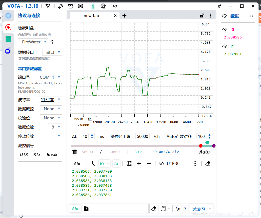
如图所示,两个通道测量值成功输出
转动电位器,输出随之变化
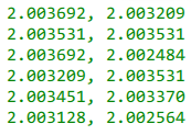
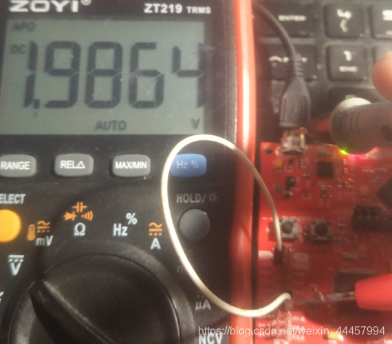
电压表实测1.9864V时,打印测量值为2.003V,误差0.8%左右