一、概述
GPIO,即通用I/O(输入/输出)端口,是STM32可控制的引脚。STM32芯片的GPIO引脚与外部设备连接起来,可实现与外部通讯、控制外部硬件或者采集外部硬件数据的功能。STM32F407有8组IO。分别为GPIOA~GPIOH,除了GPIOH只有两个IO,其余每组IO有16根引脚。
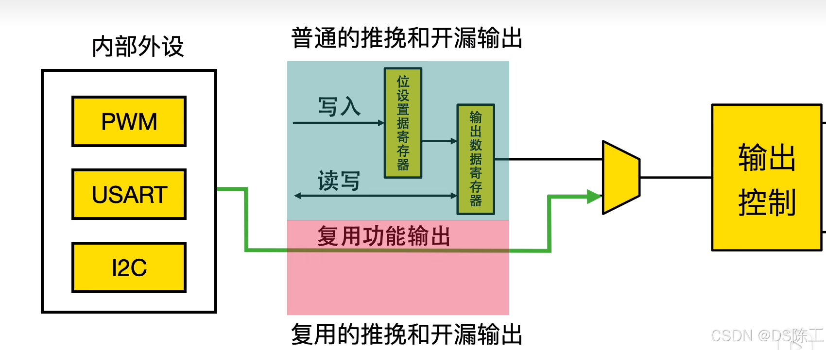
GPIO的复用:
STM32F4 有很多的内置外设,这些外设的外部引脚都是与 GPIO 共用的。也就是说,一个引脚可以有很多作用,但是默认为IO口,如果想使用一个 GPIO内置外设的功能引脚,就需要GPIO的复用,那么当这个 GPIO 作为内置外设使用的时候,就叫做复用。比如说串口就是GPIO复用为串口。
二、GPIO的工作模式
4种输入模式
(1)浮空输入(即不连接内部上下拉电阻)
浮空最大的特点就是电压的不确定性,它可能是0V,也可能是VCC,还可能是介于两者之间的某个值(最有可能). 浮空一般用来做ADC输入用,这样可以减少上下拉电阻对结果的影响.
(2)上拉输入(连接上拉电阻)
将不确定信号通过一个电阻钳位在高电平,电阻同时限流作用
(3)下拉输入(连接下拉电阻)
将不确定信号通过一个电阻钳位在低电平
(4)模拟输入
用于检测模拟信号的输入
4种输出模式
(5)开漏输出(带上拉或者下拉)
可实现电平转换,输出电平取决于上拉电阻电源
可以实现IO的线与
缺点
    高电平驱动能力差,取决于外部上拉电阻
    电平切换速率取决于外部上拉电阻,电阻越小速度越快
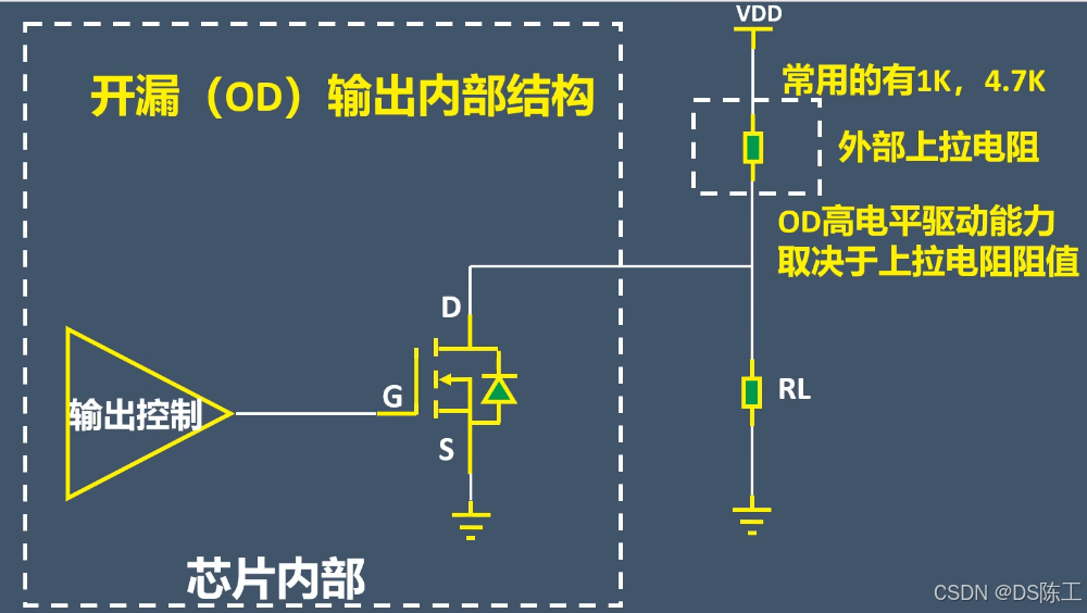
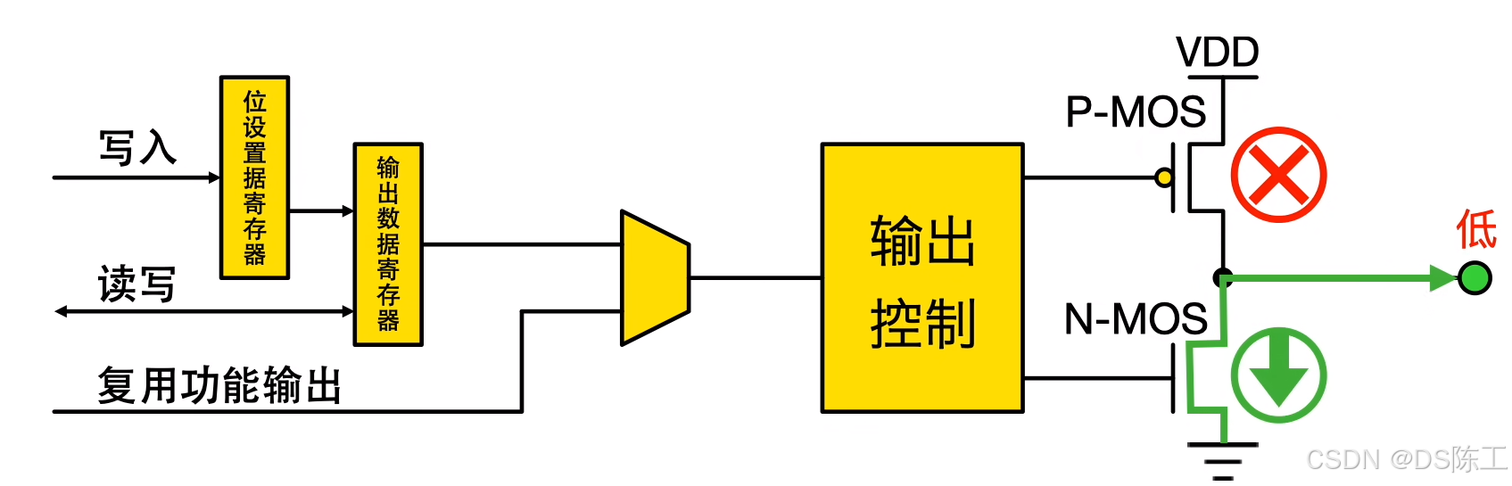
开漏输出,P-MOS永远都是截至
N-MOS导通,输出低电平
N-MOS截至
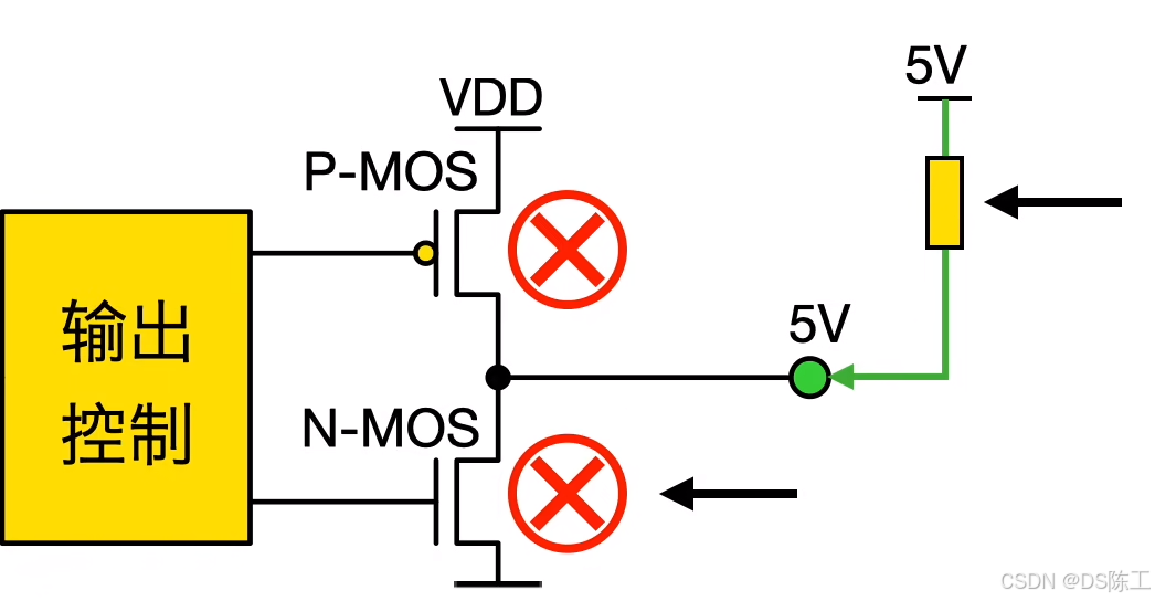
电平切换
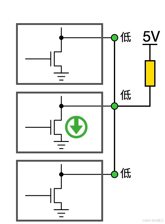
线与特性,有一个低电平,所有引脚都被拉低
(6)推挽输出(带上拉或者下拉)
输出高低电平与电源电压基本没有压差
高低电平驱动能力较强,一般数字芯片推挽输出IO口驱动电流最大可达20mA
电平切换速度快
缺点
	不支持线与
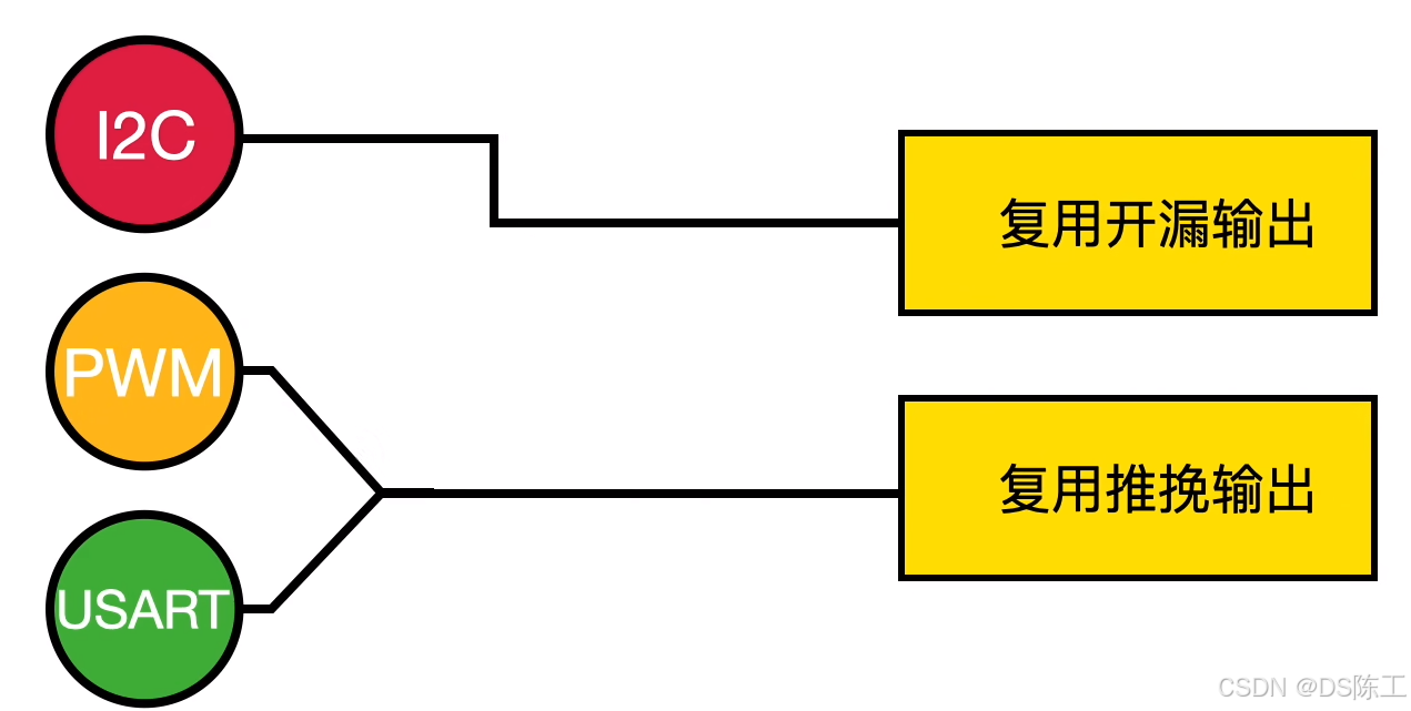
(7)复用开漏输出(带上拉或者下拉)
(8)复用推挽输出(带上拉或者下拉)
4种最大输出速度
(1)2MHZ (低速)
(2)25MHZ (中速)
(3)50MHZ (快速)
(4)100MHZ (高速)
输出配置
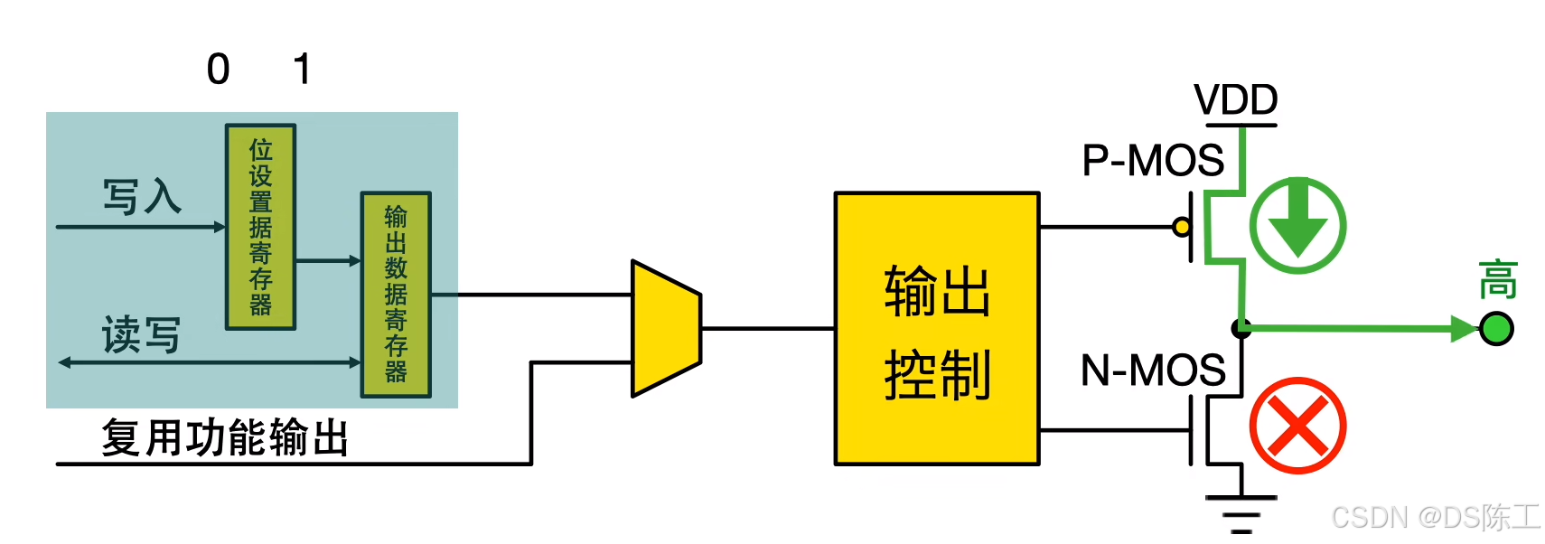
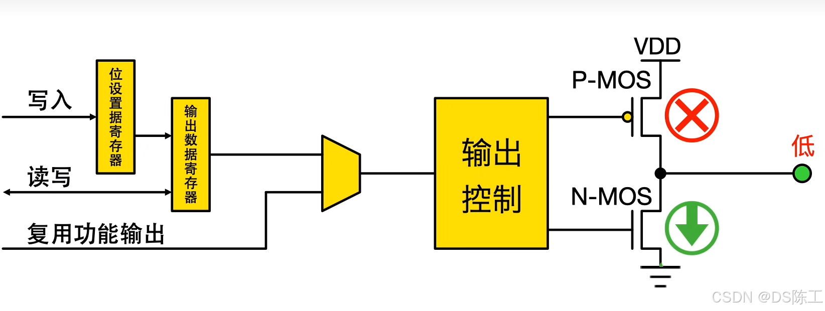
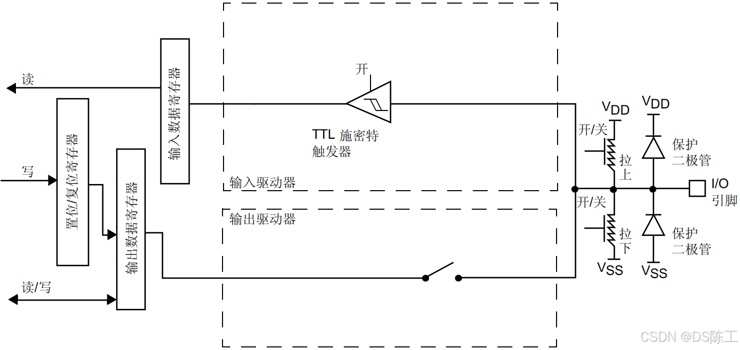
对 I/O 端口进行编程作为输出时:
- 输出缓冲器被打开:
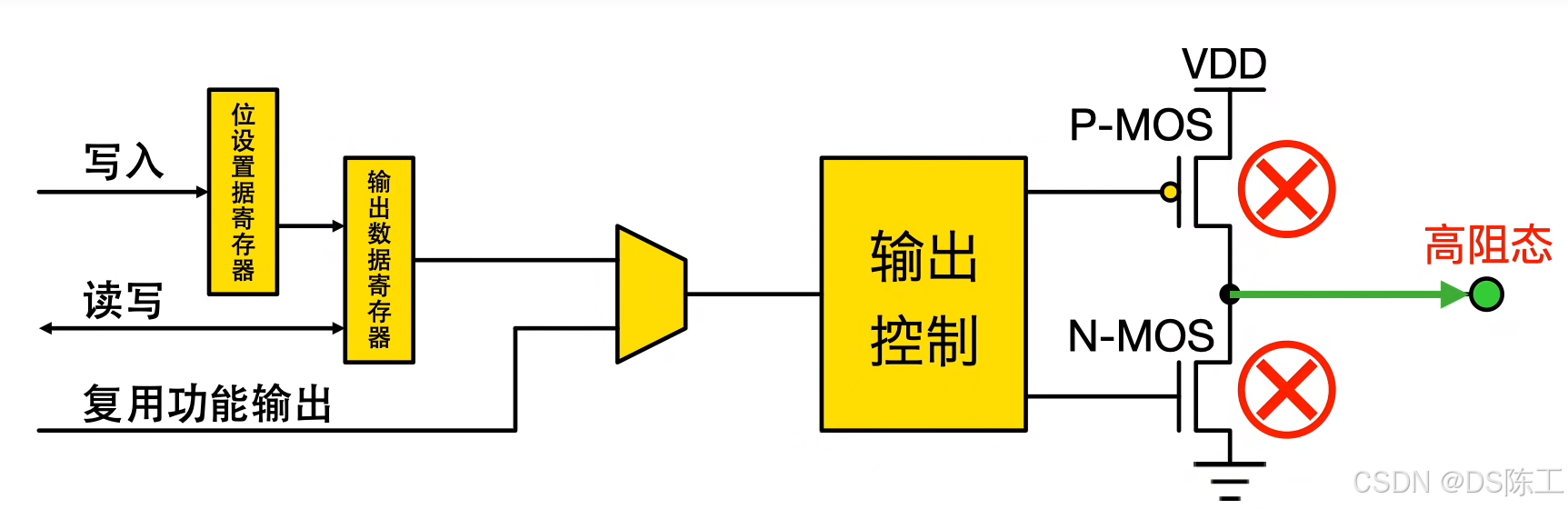
–开漏模式(常用于总线):输出寄存器中的“0”可激活 N-MOS,而输出寄存器中的“1”会使端口保持高阻态 (Hi-Z)(P-MOS 始终不激活)。
–推挽模式:输出寄存器中的“0”可激活 N-MOS,而输出寄存器中的“1”可激活P-MOS。
- 施密特触发器输入被打开
- 根据 GPIOx_PUPDR 寄存器中的值决定是否打开弱上拉电阻和下拉电阻
- 输入数据寄存器每隔 1 个 AHB1 时钟周期对 I/O 引脚上的数据进行一次采样
- 对输入数据寄存器的读访问可获取 I/O 状态
- 对输出数据寄存器的读访问可获取最后的写入值

推挽电路(push-pull)就是两个不同极性晶体管间连接的输出电路。推挽电路采用两个参数相同的功率BJT管或MOSFET管,以推挽方式存在于电路中,各负责正负半周的波形放大任务,电路工作时,两只对称的功率开关管每次只有一个导通,所以导通损耗小效率高。推挽输出既可以向负载灌电流,也可以从负载抽取电流。
在电路设计中,推挽输出是一种很常用的输出模式。推挽输出有很多优点,比如更低的损耗,更安全的输出等。“推挽”之意,即为当一个管子推出去时,另一个管子拉回来。输入不同,交替导通。
举个例子
- 当输入信号为高电平的时候,上面的管子导通,下面的管子截止,输出信号为高电平。
- 当输入信号为低电平的时候,上面的管子截止,下面的管子导通,输出信号为低电平。
MOS管
- N型mos比P型mos管使用的多
- N型mos管比P型mos管的开关速度快(工艺的影响 ),所以Pmos开关损耗多,发热严重
- Nmos比Pmos耐压高
- Nmos通过电流能力比较大,因此常用于推挽电路的下管。
输入配置
对 I/O 端口进行编程作为输入时:
- 输出缓冲器被关闭
- 施密特触发器输入被打开
- 根据 GPIOx_PUPDR 寄存器中的值决定是否打开上拉和下拉电阻
- 输入数据寄存器每隔 1 个 AHB1 时钟周期对 I/O 引脚上的数据进行一次采样
- 对输入数据寄存器的读访问可获取 I/O 状态

复用功能配置
对 I/O 端口进行编程作为复用功能时:
- 可将输出缓冲器配置为开漏或推挽
- 输出缓冲器由来自外设的信号驱动(发送器使能和数据)
- 施密特触发器输入被打开
- 根据 GPIOx_PUPDR 寄存器中的值决定是否打开弱上拉电阻和下拉电阻
- 输入数据寄存器每隔 1 个 AHB1 时钟周期对 I/O 引脚上的数据进行一次采样
- 对输入数据寄存器的读访问可获取 I/O 状态
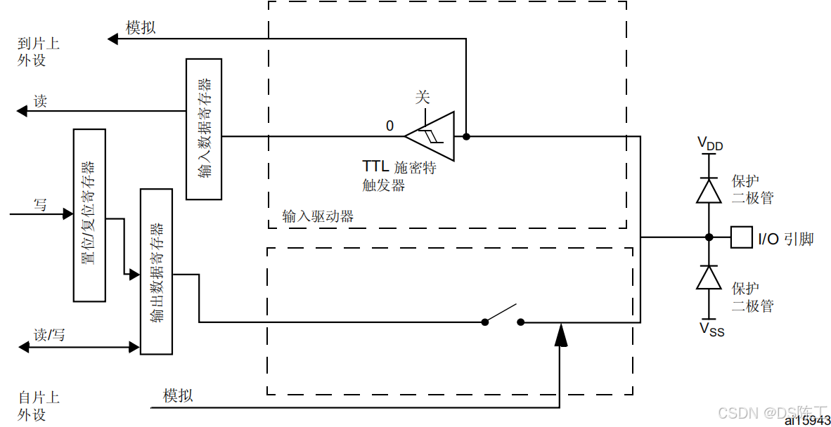
模拟配置
对 I/O 端口进行编程作为模拟配置时:
- 输出缓冲器被禁止。
- 施密特触发器输入停用,I/O 引脚的每个模拟输入的功耗变为零。施密特触发器的输出被 强制处理为恒定值 (0)。
- 弱上拉和下拉电阻被关闭。
- 对输入数据寄存器的读访问值为“0”。
在模拟配置中,I/O 引脚不能为 5 V 容忍
三、使用库函数编程技巧
-
阅读硬件原理图《中科深谷_STM32F4_原理图_V2.0.pdf》,了解当前需要使用STM32芯片哪个硬件,就可以知道使用哪些库函数接口。
-
使用库函数的时候,只需要了解该函数的使用方法,如传入参数、返回值、功能描述就足矣。库函数里面的编写内容不需要了解,这些代码都是由ST公司去实现的。
-
如何使用库函数实现一个具体的功能,ST公司都会提供例子文档,告诉我们库函数如何使用,如函数前后的调用顺序,详细硬件初始化流程,无论是新手还是老手都要看。
- STM32F4xx中文参考手册.pdf
- stm32f4xx_dsp_stdperiph_lib_um.chm
- 使用的编程标准C,也就是ANSI C编程。
四、研究库函数
库函数参考有两种方法:
1.参考库函数源码,逐步进行阅读,仅供于参考,详细如下。
=============================================================================== ##### How to use this driver ##### =============================================================================== [..] (#) Enable the GPIO AHB clock using the following function RCC_AHB1PeriphClockCmd(RCC_AHB1Periph_GPIOx, ENABLE); (#) Configure the GPIO pin(s) using GPIO_Init() Four possible configuration are available for each pin: (++) Input: Floating, Pull-up, Pull-down. (++) Output: Push-Pull (Pull-up, Pull-down or no Pull) Open Drain (Pull-up, Pull-down or no Pull). In output mode, the speed is configurable: 2 MHz, 25 MHz, 50 MHz or 100 MHz. (++) Alternate Function: Push-Pull (Pull-up, Pull-down or no Pull) Open Drain (Pull-up, Pull-down or no Pull). (++) Analog: required mode when a pin is to be used as ADC channel or DAC output. (#) Peripherals alternate function: (++) For ADC and DAC, configure the desired pin in analog mode using GPIO_InitStruct->GPIO_Mode = GPIO_Mode_AN; (+++) For other peripherals (TIM, USART...): (+++) Connect the pin to the desired peripherals' Alternate Function (AF) using GPIO_PinAFConfig() function (+++) Configure the desired pin in alternate function mode using GPIO_InitStruct->GPIO_Mode = GPIO_Mode_AF (+++) Select the type, pull-up/pull-down and output speed via GPIO_PuPd, GPIO_OType and GPIO_Speed members (+++) Call GPIO_Init() function (#) To get the level of a pin configured in input mode use GPIO_ReadInputDataBit() (#) To set/reset the level of a pin configured in output mode use GPIO_SetBits()/GPIO_ResetBits() (#) During and just after reset, the alternate functions are not active and the GPIO pins are configured in input floating mode (except JTAG pins).
2.借力帮助文档

五、函数接口
1.端口硬件时钟使能
-
/**

  - @brief  Enables or disables the AHB1 peripheral clock.
  - @note   After reset, the peripheral clock (used for registers read/write access)
  - is disabled and the application software has to enable this clock before
  - using it.
  - @param  RCC_AHBPeriph: specifies the AHB1 peripheral to gates its clock.
  - This parameter can be any combination of the following values:
  - @arg RCC_AHB1Periph_GPIOA:       GPIOA clock
  - @arg RCC_AHB1Periph_GPIOB:       GPIOB clock
  - @arg RCC_AHB1Periph_GPIOC:       GPIOC clock
  - @arg RCC_AHB1Periph_GPIOD:       GPIOD clock
  - @arg RCC_AHB1Periph_GPIOE:       GPIOE clock
  - @arg RCC_AHB1Periph_GPIOF:       GPIOF clock
  - @arg RCC_AHB1Periph_GPIOG:       GPIOG clock
  - @arg RCC_AHB1Periph_GPIOG:       GPIOG clock
  - @arg RCC_AHB1Periph_GPIOI:       GPIOI clock
  - @arg RCC_AHB1Periph_GPIOJ:       GPIOJ clock (STM32F42xxx/43xxx devices)
  - @arg RCC_AHB1Periph_GPIOK:       GPIOK clock (STM32F42xxx/43xxx devices)
  - @arg RCC_AHB1Periph_CRC:         CRC clock
  - @arg RCC_AHB1Periph_BKPSRAM:     BKPSRAM interface clock
  - @arg RCC_AHB1Periph_CCMDATARAMEN CCM data RAM interface clock
  - @arg RCC_AHB1Periph_DMA1:        DMA1 clock
  - @arg RCC_AHB1Periph_DMA2:        DMA2 clock
  - @arg RCC_AHB1Periph_DMA2D:       DMA2D clock (STM32F429xx/439xx devices)
  - @arg RCC_AHB1Periph_ETH_MAC:     Ethernet MAC clock
  - @arg RCC_AHB1Periph_ETH_MAC_Tx:  Ethernet Transmission clock
  - @arg RCC_AHB1Periph_ETH_MAC_Rx:  Ethernet Reception clock
  - @arg RCC_AHB1Periph_ETH_MAC_PTP: Ethernet PTP clock
  - @arg RCC_AHB1Periph_OTG_HS:      USB OTG HS clock
  - @arg RCC_AHB1Periph_OTG_HS_ULPI: USB OTG HS ULPI clock
  - @param  NewState: new state of the specified peripheral clock.
  - This parameter can be: ENABLE or DISABLE.
  - @retval None
  	*/
  	void RCC_AHB1PeriphClockCmd(uint32_t RCC_AHB1Periph, FunctionalState NewState)
2.GPIO的初始化
-
/**

  - @brief  Initializes the GPIOx peripheral according to the specified parameters in the GPIO_InitStruct.
  - @param  GPIOx: where x can be (A..K) to select the GPIO peripheral for STM32F405xx/407xx and STM32F415xx/417xx devices
  - x can be (A..I) to select the GPIO peripheral for STM32F42xxx/43xxx devices.
  - x can be (A, B, C, D and H) to select the GPIO peripheral for STM32F401xx devices.
  - @param  GPIO_InitStruct: pointer to a GPIO_InitTypeDef structure that contains
  - the configuration information for the specified GPIO peripheral.
  - @retval None
  */
  	void GPIO_Init(GPIO_TypeDef* GPIOx, GPIO_InitTypeDef* GPIO_InitStruct)
3.GPIO初始化结构体
/**
  * @brief   GPIO Init structure definition
  */
typedef struct
{
  uint32_t GPIO_Pin;              /*!< Specifies the GPIO pins to be configured.
                                       This parameter can be any value of @ref GPIO_pins_define */

  GPIOMode_TypeDef GPIO_Mode;     /*!< Specifies the operating mode for the selected pins.
                                       This parameter can be a value of @ref GPIOMode_TypeDef */

  GPIOSpeed_TypeDef GPIO_Speed;   /*!< Specifies the speed for the selected pins.
                                       This parameter can be a value of @ref GPIOSpeed_TypeDef */

  GPIOOType_TypeDef GPIO_OType;   /*!< Specifies the operating output type for the selected pins.
                                       This parameter can be a value of @ref GPIOOType_TypeDef */

  GPIOPuPd_TypeDef GPIO_PuPd;     /*!< Specifies the operating Pull-up/Pull down for the selected pins.
                                       This parameter can be a value of @ref GPIOPuPd_TypeDef */
}GPIO_InitTypeDef;
4.GPIO的引脚电平设置
-
设置高电平
-
/**

  - @brief  Sets the selected data port bits.
  - @note   This functions uses GPIOx_BSRR register to allow atomic read/modify
  - accesses. In this way, there is no risk of an IRQ occurring between
  - the read and the modify access.
  - @param  GPIOx: where x can be (A..K) to select the GPIO peripheral for STM32F405xx/407xx and STM32F415xx/417xx devices
  - x can be (A..I) to select the GPIO peripheral for STM32F42xxx/43xxx devices.
  - x can be (A, B, C, D and H) to select the GPIO peripheral for STM32F401xx devices.
  - @param  GPIO_Pin: specifies the port bits to be written.
  - This parameter can be any combination of GPIO_Pin_x where x can be (0..15).
  - @retval None
  */
  void GPIO_SetBits(GPIO_TypeDef* GPIOx, uint16_t GPIO_Pin)
-
-
设置低电平
-
/**

  - @brief  Clears the selected data port bits.
  - @note   This functions uses GPIOx_BSRR register to allow atomic read/modify
  - accesses. In this way, there is no risk of an IRQ occurring between
  - the read and the modify access.
  - @param  GPIOx: where x can be (A..K) to select the GPIO peripheral for STM32F405xx/407xx and STM32F415xx/417xx devices
  - x can be (A..I) to select the GPIO peripheral for STM32F42xxx/43xxx devices.
  - x can be (A, B, C, D and H) to select the GPIO peripheral for STM32F401xx devices.
  - @param  GPIO_Pin: specifies the port bits to be written.
  - This parameter can be any combination of GPIO_Pin_x where x can be (0..15).
  - @retval None
  	*/
  void GPIO_ResetBits(GPIO_TypeDef* GPIOx, uint16_t GPIO_Pin)
-
设置引脚电平,可以尝试GPIO_Write、GPIO_WriteBit函数。
-
读取某个端口引脚电平
-
/**

  - @brief  Reads the specified input port pin.
  - @param  GPIOx: where x can be (A..K) to select the GPIO peripheral for STM32F405xx/407xx and STM32F415xx/417xx devices
  - x can be (A..I) to select the GPIO peripheral for STM32F42xxx/43xxx devices.
  - x can be (A, B, C, D and H) to select the GPIO peripheral for STM32F401xx devices.
  - @param  GPIO_Pin: specifies the port bit to read.
  - This parameter can be GPIO_Pin_x where x can be (0..15).
  - @retval The input port pin value.
  	*/
  	uint8_t GPIO_ReadInputDataBit(GPIO_TypeDef* GPIOx, uint16_t GPIO_Pin)
六、LED实验
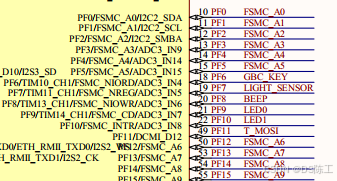
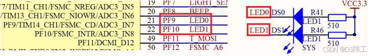
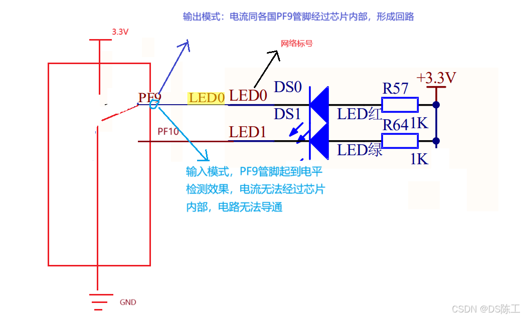
本章用到的硬件只有 LED(DS0 和 DS1)。其电路在 VSTC STM32F4 开发板
上默认是已经连接好了的。 DS0 接 PF9, DS1 接 PF10。所以在硬件上不需要动任何东西。 其连
接原理图如图 下:
-
练习1: 、
实现流水灯,每隔一段时间点亮对应一盏灯。
#include "stm32f4xx.h"

    // 定义GPIO外设
    GPIO_InitTypeDef  GPIO_InitStructure;

    void delay(void)
    {
    	int i = 0x500000;
    	while(i--);
    }

    // 初始化LED
    void init_led(void)
    {
    	// 使能F组管脚工作
    	RCC_AHB1PeriphClockCmd(RCC_AHB1Periph_GPIOF, ENABLE);

    	GPIO_InitStructure.GPIO_Mode = GPIO_Mode_OUT; // 输出模式
    	GPIO_InitStructure.GPIO_OType = GPIO_OType_PP; // 推挽模式
    	GPIO_InitStructure.GPIO_Pin = GPIO_Pin_9 | GPIO_Pin_10;
    	GPIO_InitStructure.GPIO_PuPd = GPIO_PuPd_NOPULL; // 无拉电阻
    	GPIO_InitStructure.GPIO_Speed = GPIO_High_Speed;
    	// 初始化GPIO
    	GPIO_Init(GPIOF, &GPIO_InitStructure);
    }

    int main(void)
    {
    	// 初始化LED
    	init_led();

    	while(1)
    	{
    		GPIO_ResetBits(GPIOF,GPIO_Pin_9);
    		GPIO_SetBits(GPIOF,GPIO_Pin_10);
    		delay();
    		GPIO_ResetBits(GPIOF,GPIO_Pin_10);
    		GPIO_SetBits(GPIOF,GPIO_Pin_9);
    		delay();

    	}

    }
七. 工程文件封装
1. 创建模块管理目录

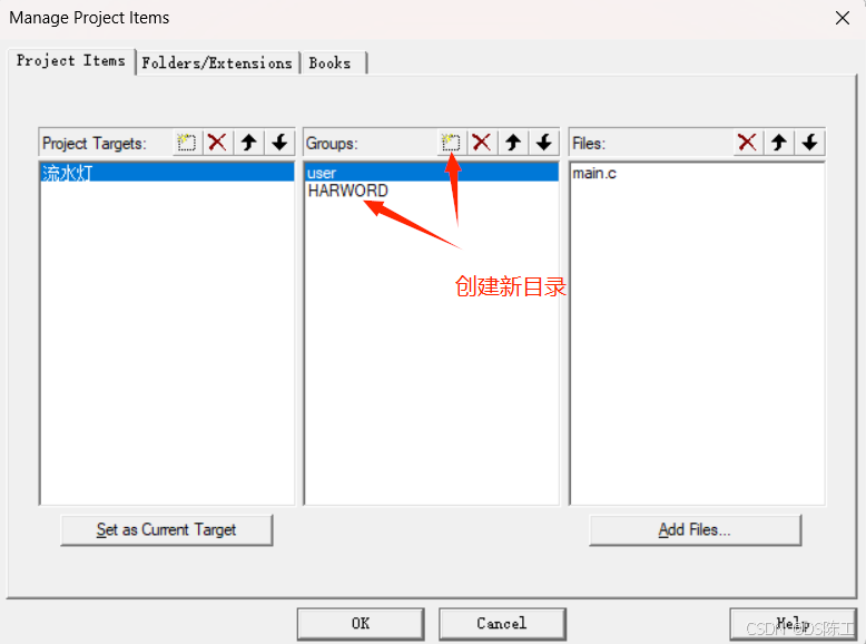
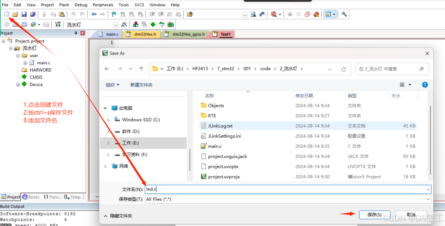
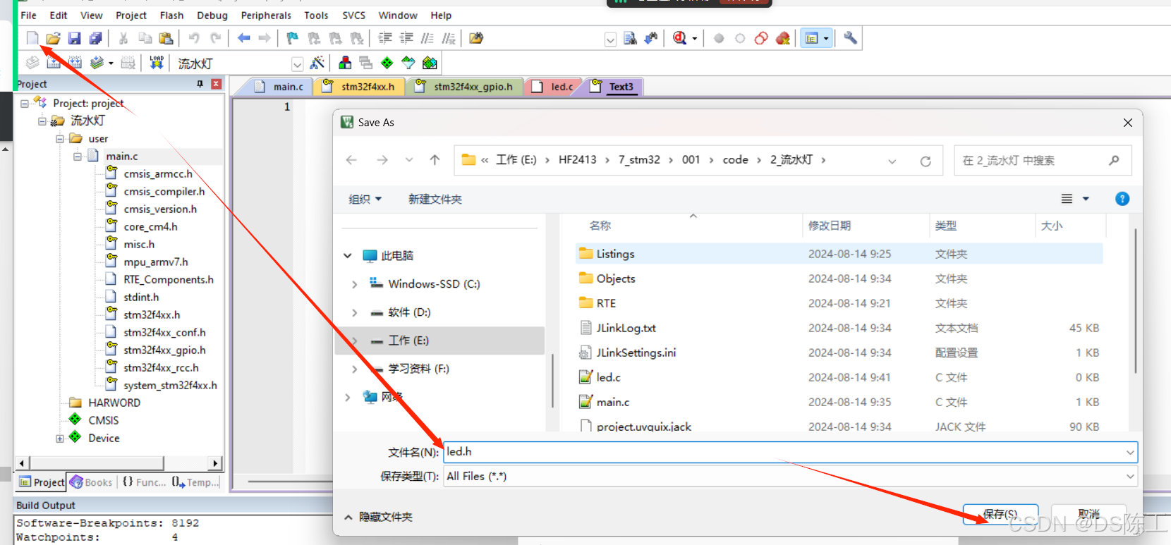
重复以上操作创建led.h文件
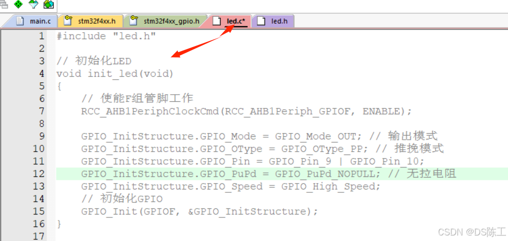
头文件添加函数声明

源文件添加模块初始化
将封装好的各模块添加到工程
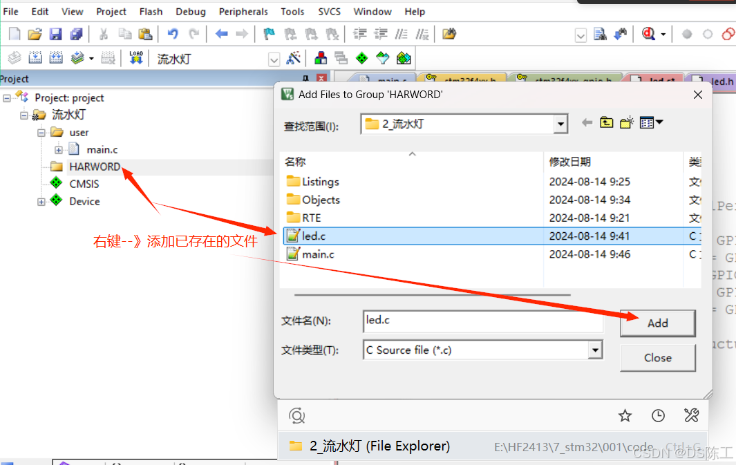
完成后如图所示

练习2
实现呼吸灯
    // led.h
    #ifndef _LED_H
    #define _LED_H

    #include "stm32f4xx.h"

    // 声明led
    void init_led(void);

    #endif
//led.c
#include "led.h"

// 初始化LED
void init_led(void)
{
	// 定义GPIO外设
	GPIO_InitTypeDef  GPIO_InitStructure;
	// 使能F组管脚工作
	RCC_AHB1PeriphClockCmd(RCC_AHB1Periph_GPIOF, ENABLE);

	GPIO_InitStructure.GPIO_Mode = GPIO_Mode_OUT; // 输出模式
	GPIO_InitStructure.GPIO_OType = GPIO_OType_PP; // 推挽模式
	GPIO_InitStructure.GPIO_Pin = GPIO_Pin_9 | GPIO_Pin_10;
	GPIO_InitStructure.GPIO_PuPd = GPIO_PuPd_NOPULL; // 无拉电阻
	GPIO_InitStructure.GPIO_Speed = GPIO_High_Speed;
	// 初始化GPIO
	GPIO_Init(GPIOF, &GPIO_InitStructure);
}
// main.c
#include "led.h"

void delay(int i)
{
	while(i--);
}

int main()
{
	init_led();

	while(1)
	{
		int count = 0x10000;
		int i ;
		// 由暗变亮
		for(i = 0; i < count; i++)
		{
			GPIO_ResetBits(GPIOF, GPIO_Pin_9|GPIO_Pin_10);
			delay(i);
			GPIO_SetBits(GPIOF, GPIO_Pin_9|GPIO_Pin_10);
			delay(count-i);
		}

		// 由亮变暗
		for(i = count; i > 0; i--)
		{
			GPIO_ResetBits(GPIOF, GPIO_Pin_9|GPIO_Pin_10);
			delay(i);
			GPIO_SetBits(GPIOF, GPIO_Pin_9|GPIO_Pin_10);
			delay(count-i);
		}

	}

}
七、蜂鸣器
- 介绍
蜂鸣器是一种一体化结构的电子讯响器,采用直流电压供电,广泛应用于计算机、打印机、复印机、报警器、电子玩具、汽车电子设备、电话机、定时器等电子产品中作发声器件。蜂鸣
器主要分为压电式蜂鸣器和电磁式蜂鸣器两种类型。
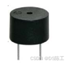
这里的有源不是指电源的“源”,而是指有没有自带震荡电路,有源蜂鸣器自带了震荡电路,
一通电就会发声;无源蜂鸣器则没有自带震荡电路,必须外部提供 2~5Khz 左右的方波驱动,
才能发声。
-
硬件设计
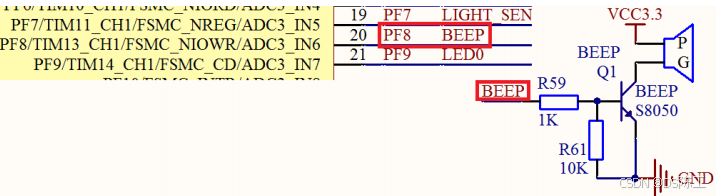
DS0 在上一章已有介绍,而蜂鸣器在硬件上也是直接连接好了的, 不需要经过任何设置,
直接编写代码就可以了。 蜂鸣器的驱动信号连接在 STM32F4 的 PF8 上 。RCC_AHB1PeriphClockCmd(RCC_AHB1Periph_GPIOF, ENABLE); // 初始化蜂鸣器 GPIO_InitStructure.GPIO_Mode = GPIO_Mode_OUT;// 输出模式 GPIO_InitStructure.GPIO_OType = GPIO_OType_PP;// 推挽 GPIO_InitStructure.GPIO_Pin = GPIO_Pin_8; //GPIO_InitStructure.GPIO_PuPd = GPIO_PuPd_DOWN; GPIO_InitStructure.GPIO_Speed = GPIO_Speed_100MHz; GPIO_Init(GPIOF, &GPIO_InitStructure); while(1) { // 低电平响 GPIO_ResetBits(GPIOF, GPIO_Pin_8); //GPIO_SetBits(GPIOF,GPIO_Pin_8); }
八、按键
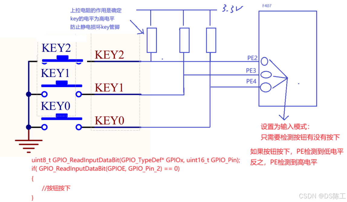
STM32F4 开发板上载有的 4 个按钮(KEY_UP、KEY0、 KEY1 和 KEY2),按键 KEY0 连接在 PE4 上、 KEY1 连接在 PE3 上、 KEY2 连接在 PE2 上、 KEY_UP,连接在 PA0 上 。

这里需要注意的是: KEY0、 KEY1 和 KEY2 是低电平有效的,而 KEY_UP 是高电平有效
的, 并且外部都没有上下拉电阻,所以,需要在 STM32F4 内部设置上下拉。
作业:
按一下key_up蜂鸣器响,再按一次停止
按key0红灯亮,再按一次灭
按key1绿灯亮,再按一次灭
按key2红绿灯亮,再按一次灭
九、应用领域
1.常见密码锁,矩阵键盘